ALLPCB


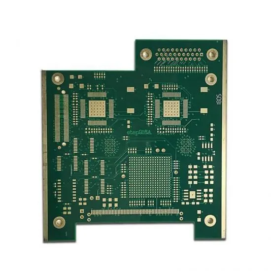
In the world of electronics, multilayer PCBs (Printed Circuit Boards) are the backbone of complex devices, enabling compact designs with high functionality. However, achieving optimal performance and stability in these boards requires careful attention to copper balancing. But what exactly is copper balancing in multilayer PCBs, and why does it matter? Simply put, copper balancing refers to the even distribution of copper across the layers of a PCB to prevent warping, ensure structural stability, and maintain signal integrity. In this comprehensive guide, we’ll dive deep into the importance of copper balancing, techniques to achieve it, and how it impacts PCB stackup, warping prevention, and signal integrity for superior performance.
What Is Copper Balancing in Multilayer PCBs?
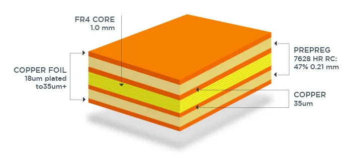
Multilayer PCBs consist of multiple layers of copper and insulating materials stacked together to form a compact and efficient circuit board. Each layer often has a different copper pattern based on the design’s requirements, such as power planes, ground planes, or signal traces. Copper balancing is the practice of distributing copper evenly across these layers to avoid mechanical stress and maintain uniformity during manufacturing and operation.
Uneven copper distribution can lead to issues like warping or twisting of the board, especially during the high-temperature processes of PCB fabrication, such as lamination and soldering. When copper is unevenly spread, the board’s layers expand and contract at different rates, causing physical deformation. This not only affects the board’s structural integrity but also disrupts signal integrity, leading to performance issues in high-speed circuits.
Why Copper Balancing Matters for Stability and Performance
Copper balancing plays a critical role in ensuring both the mechanical stability and electrical performance of multilayer PCBs. Let’s break down its importance in key areas:
1. Preventing Warping and Mechanical Stress
During PCB manufacturing, layers are bonded together under heat and pressure. If copper distribution is uneven—say, one layer has 70% copper coverage while another has only 20%—the layers will experience different levels of thermal expansion. This mismatch can cause the board to warp or twist, leading to potential failures during assembly or operation. Warping can also make it difficult to mount components accurately, affecting the overall reliability of the device.
2. Enhancing Signal Integrity
In high-speed designs, signal integrity is paramount. Uneven copper distribution can create impedance mismatches, leading to signal reflections and crosstalk. For example, in a 4-layer PCB stackup designed for a 5 GHz signal, an unbalanced copper layout might result in impedance deviations of up to 10 ohms from the target value of 50 ohms. This can degrade signal quality, causing data errors or reduced performance in applications like telecommunications or computing.
3. Improving Thermal Management
Copper is an excellent conductor of heat. Balanced copper distribution helps dissipate heat evenly across the board, preventing hotspots that could damage components or degrade performance. For instance, in power electronics, a well-balanced PCB can reduce thermal stress on critical components, extending their lifespan.
Techniques for Achieving Copper Balancing in Multilayer PCBs
Achieving copper balancing requires careful planning during the design and manufacturing stages. Below are some proven techniques to ensure uniformity and stability in multilayer PCB designs:
1. Symmetrical PCB Stackup Design
A symmetrical stackup is the foundation of copper balancing. This means arranging layers in a way that mirrors copper distribution on both sides of the board’s centerline. For example, in an 8-layer PCB, if layer 1 (top) has a dense copper pattern, layer 8 (bottom) should have a similar density. Similarly, inner layers like layer 2 and layer 7 should be balanced. This symmetry minimizes stress during thermal cycles.
A typical 4-layer stackup for balanced design might look like this:
- Layer 1: Signal (50% copper coverage)
- Layer 2: Ground Plane (80% copper coverage)
- Layer 3: Power Plane (80% copper coverage)
- Layer 4: Signal (50% copper coverage)
This arrangement ensures that opposing layers have similar copper densities, reducing the risk of warping.
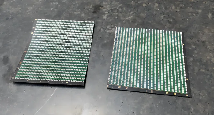
2. Use of Copper Thieving
Copper thieving is a fabrication technique where small, non-functional copper dots or patterns are added to areas of the PCB with low copper density. These patterns do not connect to any circuit but help balance the copper coverage across the layer. For instance, if a signal layer has only 30% copper due to sparse traces, adding thieving patterns can increase coverage to 60-70%, matching adjacent layers. This technique also aids in uniform plating during manufacturing, preventing over-etching or under-etching.
3. Dummy Copper Fills
Similar to copper thieving, dummy copper fills involve adding non-functional copper areas to balance density. However, unlike thieving, which uses isolated dots, dummy fills can be larger shapes or grids. These fills are often used on outer layers to match the copper percentage of inner planes, ensuring mechanical stability.
4. Panel-Level Balancing
During manufacturing, multiple PCBs are often fabricated on a single panel. Copper balancing should extend to the entire panel, not just individual boards. Designers can add dummy patterns or balance bars to unused areas of the panel to ensure uniform copper distribution, reducing stress across the entire sheet.
Copper Balancing for Warping Prevention
Warping is one of the most common issues in multilayer PCB manufacturing, and it’s directly tied to copper imbalance. When layers have significantly different copper densities, the board can bend or twist as it cools after lamination or reflow soldering. Here’s how copper balancing helps prevent warping:
- Uniform Thermal Expansion: Balanced copper ensures that all layers expand and contract at similar rates during heating and cooling cycles. For example, maintaining copper coverage within a 10-15% difference between layers can significantly reduce warping risks.
- Reduced Mechanical Stress: Even copper distribution minimizes internal stresses that could deform the board. This is especially critical for thin PCBs (e.g., 0.8 mm thick) used in portable devices.
- Improved Lamination: During the lamination process, balanced copper prevents uneven pressure distribution, ensuring a flat and stable board.
To quantify the impact, studies have shown that boards with copper coverage differences of more than 20% between adjacent layers are up to 50% more likely to exhibit warping during manufacturing. By adhering to strict balancing guidelines, manufacturers can achieve flatness tolerances as low as 0.0075 inches per inch, meeting industry standards for high-reliability applications.
Impact of Copper Balancing on Signal Integrity
In high-speed and high-frequency designs, signal integrity is a top priority. Copper balancing directly influences how signals propagate through the PCB, affecting performance in the following ways:
1. Consistent Impedance Control
Impedance control is critical for maintaining signal quality in multilayer PCBs. Balanced copper layers ensure uniform dielectric thickness and consistent trace impedance. For instance, a target impedance of 50 ohms for a differential pair can be maintained more easily when ground and power planes have similar copper coverage, providing a stable reference.
2. Reduced Crosstalk and EMI
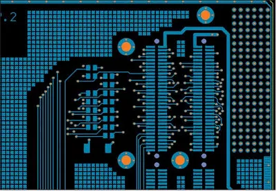
Uneven copper distribution can lead to electromagnetic interference (EMI) and crosstalk between adjacent traces. Balanced layers, especially ground planes, act as shields, minimizing noise coupling. For example, in a 6-layer PCB, ensuring that ground planes on layers 2 and 5 have at least 80% copper coverage can reduce crosstalk by up to 30% in high-speed signals.
3. Minimized Signal Reflections
Signal reflections occur when there’s an impedance mismatch along a transmission line. Balanced copper distribution helps maintain consistent impedance, reducing reflections and ensuring clean signal transmission. This is vital for applications like DDR4 memory interfaces, where signal speeds can exceed 3.2 Gbps.
Best Practices for Copper Balancing in PCB Design
To achieve optimal copper balancing in multilayer PCBs, designers and engineers should follow these best practices:
- Plan Stackup Early: Define the PCB stackup during the initial design phase, ensuring symmetry in layer arrangement and copper density.
- Use Design Software Tools: Leverage PCB design software with features to analyze copper coverage and highlight imbalances before fabrication.
- Collaborate with Manufacturers: Work closely with your fabrication partner to understand their copper balancing requirements and panelization constraints.
- Validate with Simulations: Run thermal and mechanical simulations to predict potential warping or stress points caused by copper imbalance.
- Adhere to Industry Standards: Follow guidelines like IPC-6012 for PCB flatness and copper distribution to ensure reliability.
Challenges in Copper Balancing and How to Overcome Them
While copper balancing is essential, it’s not without challenges. Dense designs with complex routing often make it difficult to achieve perfect symmetry. Additionally, cost constraints may limit the use of extra copper for thieving or dummy fills. Here are some common challenges and solutions:
- Challenge: Limited Space for Dummy Copper
Solution: Use smaller thieving patterns or distribute dummy fills in non-critical areas without affecting signal routing. - Challenge: High-Density Designs
Solution: Prioritize balancing in critical layers (e.g., ground and power planes) while allowing slight imbalances in less critical signal layers. - Challenge: Cost Constraints
Solution: Optimize copper balancing techniques during the design phase to minimize material waste and additional fabrication steps.
Conclusion: The Path to Stable and High-Performing Multilayer PCBs
Copper balancing in multilayer PCBs is a critical factor in achieving mechanical stability, preventing warping, and ensuring signal integrity for high-performance applications. By adopting techniques like symmetrical stackup design, copper thieving, and dummy fills, designers can create boards that withstand the rigors of manufacturing and operation. Whether you’re working on a 4-layer board for a consumer device or a 12-layer PCB for industrial equipment, prioritizing copper balancing will lead to better reliability and performance.
At ALLPCB, we understand the intricacies of multilayer PCB design and manufacturing. Our expertise and advanced tools help engineers achieve optimal copper balancing for every project, ensuring top-notch quality and efficiency. Start incorporating these practices into your designs today to build robust, high-performing PCBs that meet the demands of modern electronics.