 ALLPCB


In the world of electronics manufacturing, double-sided SMT assembly has become a go-to method for creating compact, high-performance printed circuit boards (PCBs). But what exactly is double-sided SMT, and why is it so widely used? Simply put, double-sided SMT (Surface Mount Technology) involves placing and soldering components on both sides of a PCB, maximizing space and functionality. This approach offers significant benefits like smaller board sizes and improved circuit density, but it also comes with challenges such as complex assembly processes and potential soldering issues.
In this comprehensive guide, we’ll dive deep into the advantages and hurdles of double-sided SMT assembly, exploring key aspects like component placement on both sides of a PCB, reflow soldering for double-sided boards, wave soldering techniques, and adhesive component mounting. Whether you’re an engineer designing a new product or a manufacturer looking to optimize production, this blog will provide actionable insights to help you navigate the world of double-sided SMT.
What Is Double-Sided SMT Assembly?
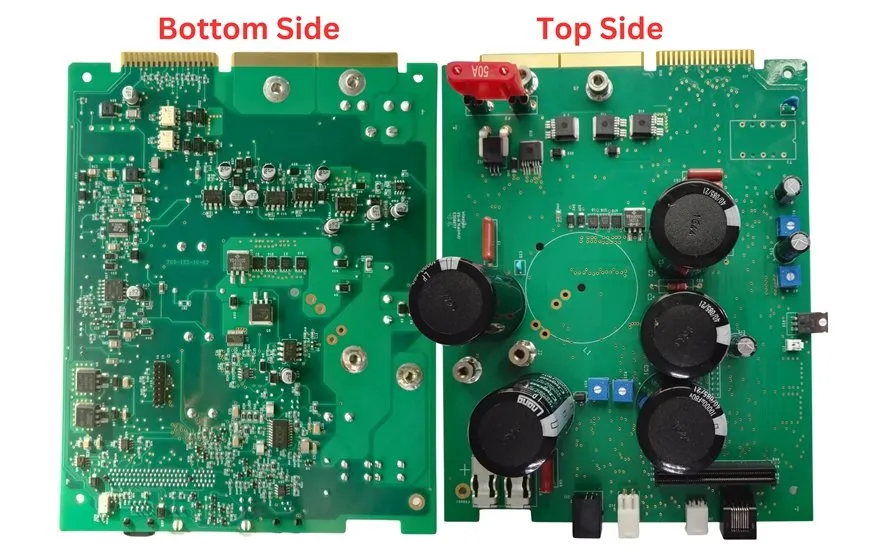
Double-sided SMT assembly is a manufacturing process where surface-mount components are placed and soldered onto both the top and bottom layers of a PCB. Unlike single-sided assembly, which uses only one side of the board, this method doubles the available space for components, allowing for more complex and compact designs. It’s a popular choice in industries like consumer electronics, automotive, and telecommunications, where space-saving and high functionality are critical.
The process typically involves applying solder paste to both sides of the board, placing components using automated pick-and-place machines, and soldering them through methods like reflow soldering for double-sided boards or wave soldering for double-sided assemblies with mixed technology (SMT and through-hole components). While this approach sounds straightforward, it requires precise planning and execution to avoid issues like component misalignment or solder joint defects.
Key Benefits of Double-Sided SMT Assembly
Double-sided SMT assembly offers several advantages that make it a preferred choice for modern electronics. Let’s explore these benefits in detail to understand why this method is so valuable.
1. Increased Circuit Density and Space Efficiency
One of the most significant advantages of double-sided SMT is the ability to place components on both sides of the PCB. This effectively doubles the available real estate for mounting components without increasing the board’s physical size. For example, in compact devices like smartphones or wearable tech, where every millimeter counts, this space efficiency can be a game-changer. By utilizing both sides, designers can pack more functionality into smaller footprints, supporting the trend toward miniaturization in electronics.
2. Enhanced Design Flexibility
With components on both sides, engineers have greater flexibility to design complex circuits. This is especially useful for high-density applications where multiple functions need to coexist on a single board. For instance, a PCB for a wireless device might have RF components on one side and digital processing components on the other, reducing interference and optimizing signal integrity. Double-sided SMT allows for creative layouts that meet specific performance requirements, such as maintaining impedance values around 50 ohms for high-speed signals in communication devices.
3. Cost-Effective for High-Volume Production
While the initial setup for double-sided SMT assembly can be complex, it often proves cost-effective in high-volume production. By fitting more components onto a single board, manufacturers can reduce the number of boards needed for a project, lowering material and assembly costs over time. Additionally, automated assembly processes like pick-and-place and reflow soldering for double-sided boards streamline production, reducing labor expenses.
4. Improved Performance for High-Speed Applications
Double-sided SMT can enhance the performance of high-speed circuits by allowing shorter trace lengths and better component placement on both sides of the PCB. Shorter traces reduce signal delay and minimize electromagnetic interference (EMI), which is critical for applications like data transmission with speeds exceeding 10 Gbps. This layout strategy helps maintain signal integrity and supports reliable operation in demanding environments.
Challenges of Double-Sided SMT Assembly
Despite its many benefits, double-sided SMT assembly comes with a set of challenges that require careful consideration during design and manufacturing. Below, we’ll break down the most common obstacles and discuss how they impact the process.
1. Complexity in Component Placement on Both Sides of PCB
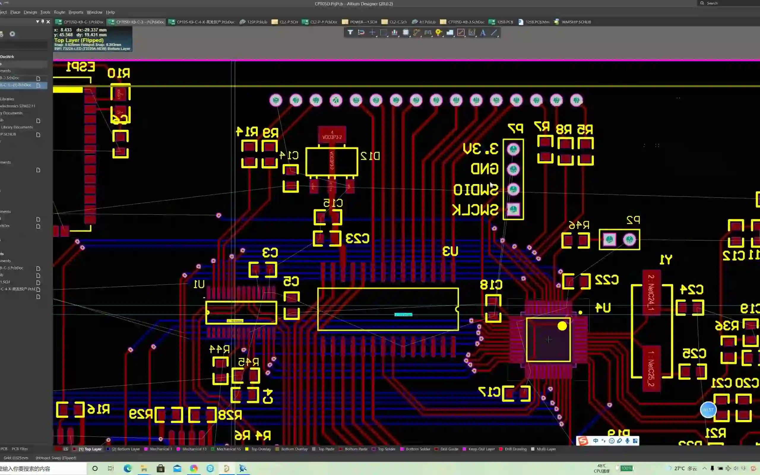
Placing components on both sides of a PCB introduces significant complexity. Designers must ensure that components on one side don’t interfere with those on the other, both physically and electrically. For example, tall components on the bottom side might create clearance issues during assembly or operation. Additionally, precise alignment is crucial to avoid misalignment during automated placement, which can lead to defective boards. This challenge often requires advanced software tools for layout planning and simulation to optimize component placement on both sides of the PCB.
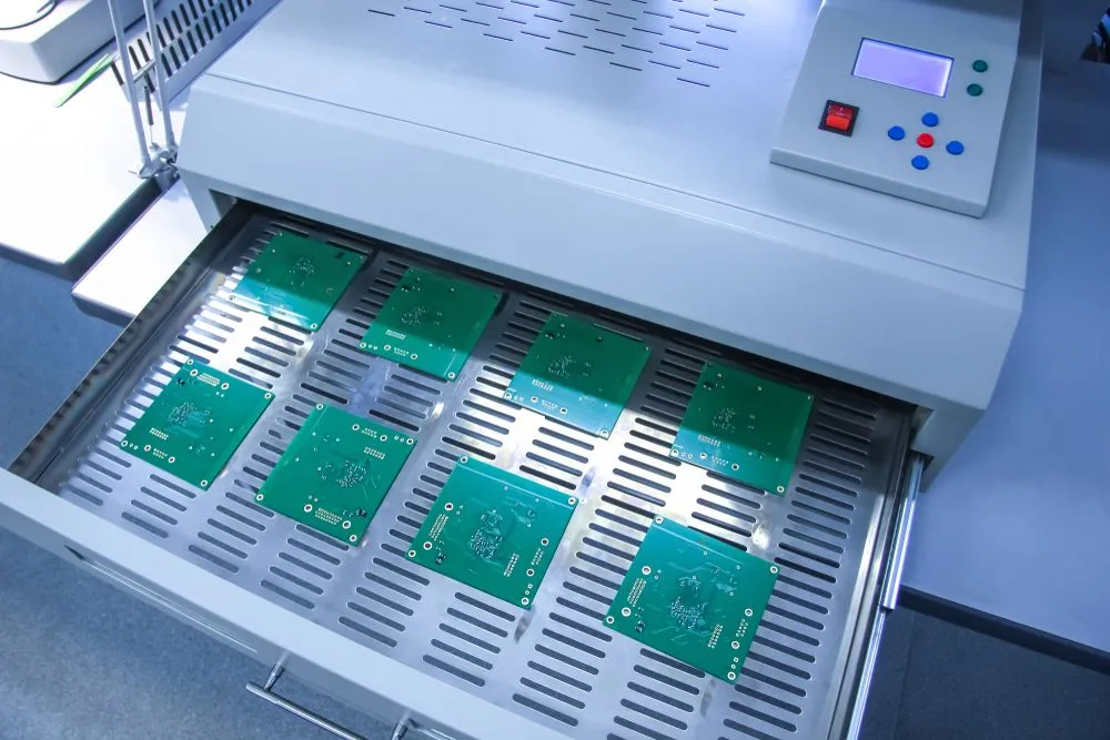
2. Soldering Challenges with Reflow Soldering for Double-Sided Boards
Reflow soldering for double-sided boards is a widely used technique, but it poses unique challenges. The process typically involves soldering one side of the board first, then flipping it to solder the other side. During the second reflow cycle, the components on the first side are exposed to high temperatures again (often around 240-260°C for lead-free solder), which can cause solder joints to weaken or components to shift if not secured properly. To mitigate this, manufacturers often use adhesives for component mounting or adjust reflow profiles to minimize thermal stress.
3. Limitations of Wave Soldering for Double-Sided Assemblies
Wave soldering for double-sided boards is another option, particularly for mixed-technology PCBs with through-hole components. However, this method is less common for pure SMT assemblies because it can remelt solder on the first side, leading to defects. Protecting the already-soldered side during wave soldering often requires masking or other protective measures, adding time and cost to the process. For many modern designs with fine-pitch SMT components, wave soldering is impractical due to the risk of bridging or uneven solder distribution.
4. Adhesive Component Mounting Issues
In double-sided SMT assembly, adhesive component mounting is sometimes used to secure components on the bottom side before the second reflow cycle. While this technique helps prevent components from falling off due to gravity or thermal stress, it introduces additional steps and costs. The adhesive must be carefully applied to avoid interfering with solder joints, and it needs to withstand high reflow temperatures without degrading. Improper adhesive application can lead to weak bonds or contamination, affecting the reliability of the final product.
5. Increased Risk of Defects and Quality Control Needs
With components on both sides, the risk of defects like tombstoning (where components stand upright due to uneven soldering) or cold solder joints increases. Inspecting double-sided boards also becomes more complex, often requiring advanced automated optical inspection (AOI) systems to check both sides for alignment and solder quality. For instance, a misalignment of just 0.1 mm in component placement can cause connection failures in fine-pitch components like 0402 resistors. Robust quality control measures are essential to ensure reliability, adding to production time and cost.
Best Practices for Successful Double-Sided SMT Assembly
To overcome the challenges of double-sided SMT assembly, following best practices during design and manufacturing is essential. These tips can help ensure a smooth process and high-quality results.
1. Optimize Component Placement on Both Sides of PCB
Carefully plan the layout to balance component placement on both sides of the PCB. Place heavier or taller components on the top side to avoid clearance issues, and group similar components together to simplify assembly. Use design software to simulate thermal and mechanical stress, ensuring that components on one side don’t affect the other. For high-speed designs, keep critical signal paths short (ideally under 10 mm for signals above 1 GHz) to maintain performance.
2. Use Appropriate Soldering Techniques
For most double-sided SMT projects, reflow soldering is the preferred method. To prevent issues during the second reflow cycle, use a lower peak temperature (e.g., 230°C instead of 260°C) if possible, and secure bottom-side components with adhesive if needed. If wave soldering for double-sided boards is required, protect the first side with a temporary mask or fixture to avoid remelting solder joints. Selecting the right soldering technique based on component types and board design is key to success.
3. Select Reliable Adhesive for Component Mounting
When adhesive component mounting is necessary, choose a high-quality, heat-resistant adhesive that can withstand reflow temperatures without breaking down. Apply it precisely using automated dispensing equipment to avoid excess adhesive that could interfere with soldering. Test the adhesive under production conditions to confirm its effectiveness, as a weak bond could lead to component displacement during assembly.
4. Implement Thorough Inspection and Testing
Invest in advanced inspection tools like AOI and X-ray systems to check solder joints and component alignment on both sides of the PCB. Conduct electrical testing to verify signal integrity and functionality, especially for high-density boards with impedance-controlled traces (e.g., maintaining 50 ohms ±10% for RF applications). Regular testing throughout the assembly process helps catch defects early, reducing rework costs.
Applications of Double-Sided SMT Assembly
Double-sided SMT assembly is used across various industries due to its ability to support compact, high-performance designs. Some common applications include:
- Consumer Electronics: Smartphones, tablets, and wearables rely on double-sided SMT to fit complex circuitry into small spaces.
- Automotive Systems: Control units and sensors use double-sided boards for reliable performance in harsh environments.
- Medical Devices: Portable diagnostic equipment benefits from the compact size and high functionality of double-sided SMT.
- Telecommunications: High-speed networking equipment uses double-sided layouts to manage dense signal paths with minimal interference.
These applications highlight the versatility of double-sided SMT assembly in meeting the demands of modern technology.
Conclusion: Weighing the Pros and Cons of Double-Sided SMT
Double-sided SMT assembly offers undeniable benefits, from increased circuit density and design flexibility to cost savings in high-volume production. However, it also presents challenges like complex component placement on both sides of the PCB, soldering difficulties with reflow and wave soldering for double-sided boards, and the need for precise adhesive component mounting. By understanding these factors and following best practices, manufacturers and designers can harness the full potential of double-sided SMT to create reliable, high-performing electronics.
At ALLPCB, we specialize in providing tailored solutions for double-sided SMT assembly, ensuring precision and quality at every step. Whether you’re working on a compact consumer device or a complex industrial system, our expertise can help bring your vision to life. Explore our services to see how we can support your next project with cutting-edge PCB assembly techniques.


