ALLPCB


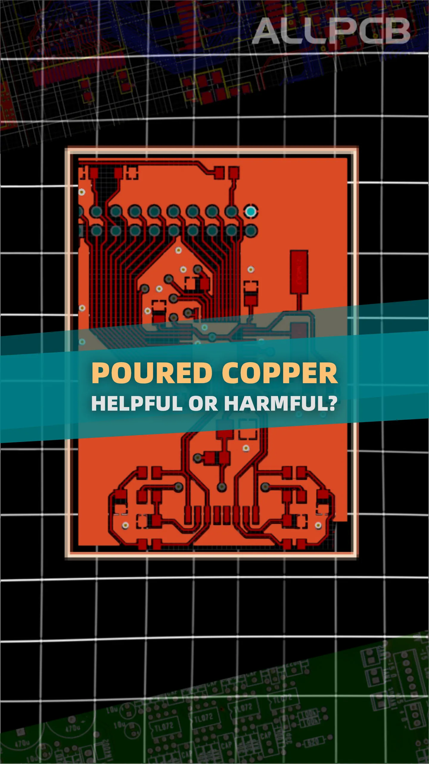
Introduction: A Customer’s Misunderstanding
A customer once asked our engineers: “If we reduce copper pour in the PCB design, doesn’t that mean less plating area, lower consumption, and therefore lower cost?”

At first glance, this logic sounds reasonable. But in reality, less copper pour in PCB does not mean saving money—in fact, it often creates serious quality issues and higher hidden costs.
At ALLPCB, our engineers explain why proper PCB copper pour is critical and how our professional solutions solve the problems caused by empty copper areas.
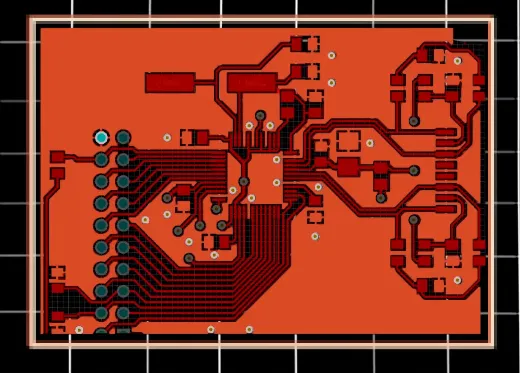
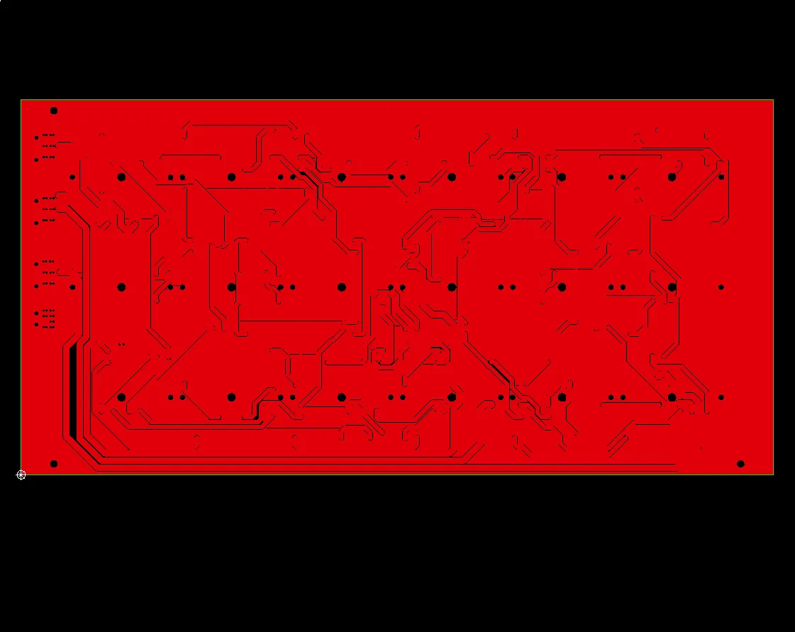
1.What is Copper Pour in PCB?
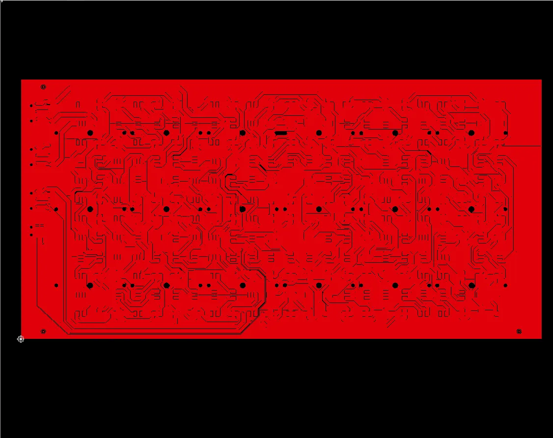
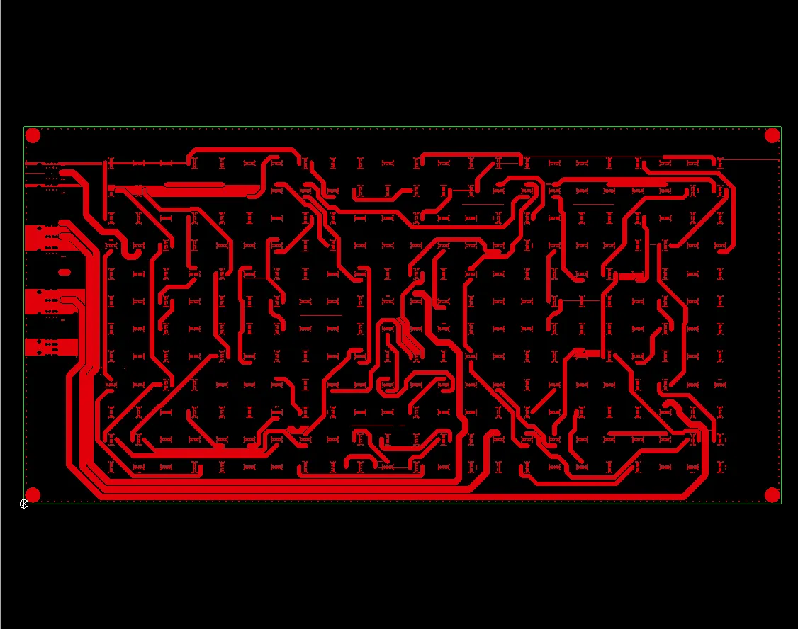
Copper pour refers to the practice of filling unused PCB areas with copper instead of leaving them blank. It can be in the form of solid copper, hatched grids, or dummy copper connections. As an indepensible part of PCB design, copper pour can be placed through various PCB design tools, like KiCad, EasyEDA. Beyond simple “filling,” copper pouring serves as an engineering technique to balance plating, control impedance, improve heat dissipation, and enhance board stability.
2.Why Do We Need Copper Pour?
- Uniform plating: balances current distribution during electroplating.
- Thermal performance: improves heat spreading and reduces hotspots.
- Mechanical stability: prevents warpage, curl, and board deformation.
- Signal integrity: provides better grounding and noise shielding.
- Connector reliability: ensures thickness uniformity in critical areas like gold fingers.
3.What Happens If You Skip Copper Pour? – Problems & ALLPCB Solutions
(A) Outer Layer Issues
1.Copper Thickness Unevenness
Without proper copper pour PCB design, the exposed copper area during plating becomes too small or unevenly distributed. Current density will not be balanced, leading to thicker plating in small areas. For example, when aiming for 1oz copper, some traces may unintentionally reach 2oz or more. This causes impedance mismatch, excessive pad thickness, and even etching difficulty.
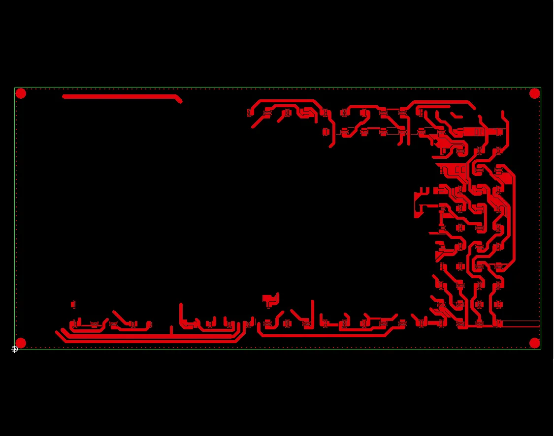
ALLPCB solution: Our engineers recommend using dummy copper fill or grid-style copper pouring in empty zones. By connecting isolated islands to a larger copper plane or ground, plating current is distributed evenly. The result is consistent copper thickness and stable electrical performance.
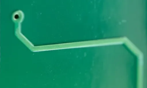
2.False Exposed Copper / Yellowing on Isolated Traces
According to our factory's feedback, there is a issue resulting from less copper pour in PCB outer layer. That's because when isolated traces are surrounded by low copper density, they receive excessive plating. During solder mask printing, constant squeegee pressure makes the ink layer thinner on these raised traces. This leads to false “exposed copper” or yellowish appearance.
ALLPCB solution: Our engineers suggest designing copper balance around isolated lines. If isolated traces cannot be avoided, increase spacing width, or apply dummy copper nearby to prevent excessive plating.
3.Film Trapping
Sometimes we may observe black spots or discoloration between lines under a microscope, that is what we called "trapped film". If line-to-line spacing is too narrow (e.g., only 4–5 mil), photoresist residue may remain between them after exposure and development.
ALLPCB solution: ALLPCB advises customers to avoid long isolated lines and instead apply copper pour in blank regions. If spacing must be tight, design adjustments or widening trace gaps reduce the risk of trapped film.
4.Board Warpage / Curl
Oue cusotmers sometimes have a question that why does the PCB warp or curl after reflow. This often results from uneven copper distribution on outer layers, causing different expansion/contraction rates under thermal cycling, which pulls the board and leads to deformation.
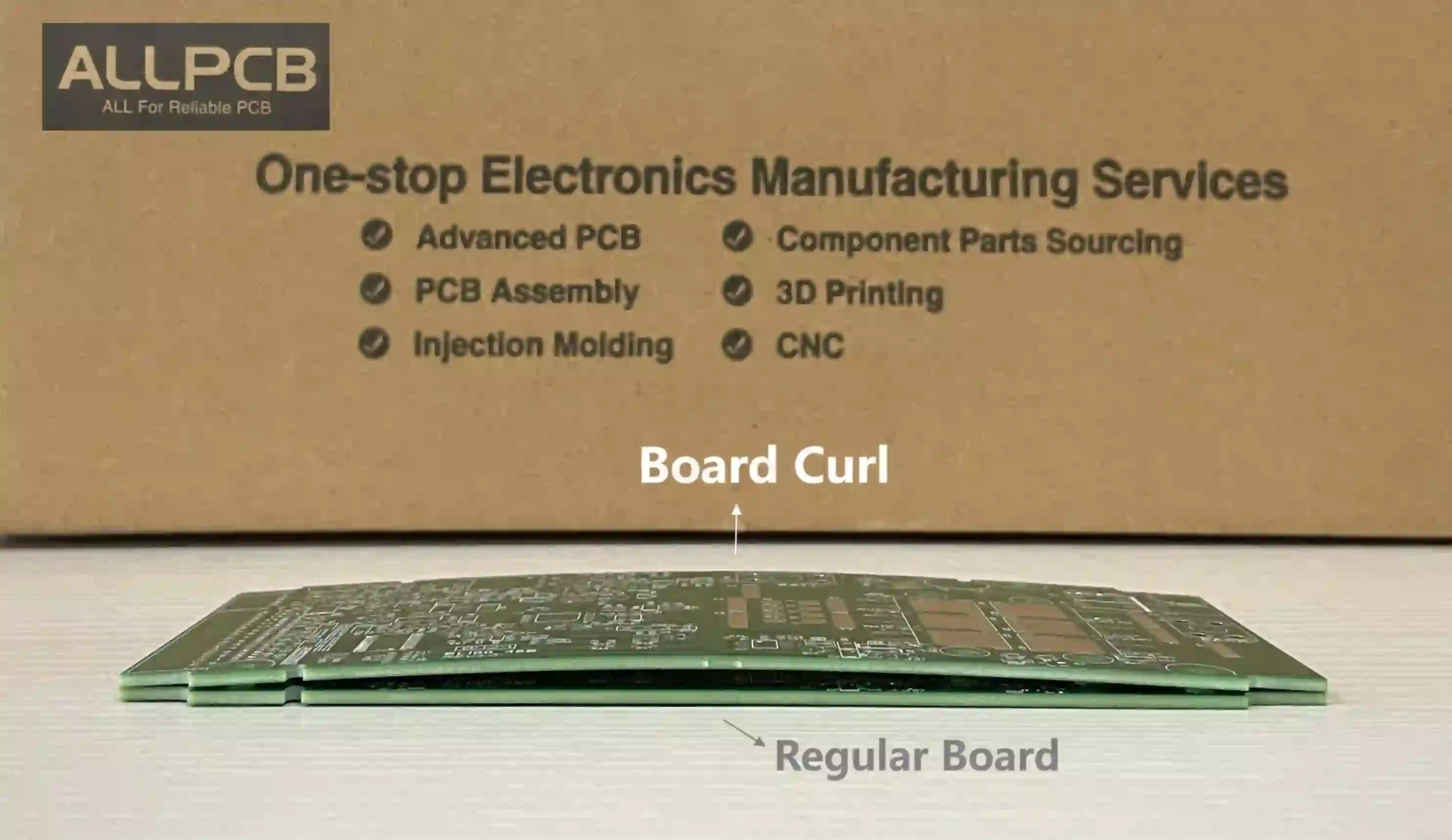
ALLPCB solution: According to our engineers' suggestion, we tend to balance copper distribution by adding copper fill to empty areas at the very beggining of design. We also recommend high Tg, low CTE materials for better thermal stability. Meanwhile, optimizing reflow temperature profiles also helps a lot.
(B) Inner Layer Issues
1.Local Overheating
Skipping copper pour PCB designs in high-speed or high-current boards reduces heat dissipation, leading to localized hotspots and shorter component lifespan.
ALLPCB solution: ALLPCB engineers design balanced copper planes as “heat spreaders.” This ensures even thermal performance and protects sensitive devices.
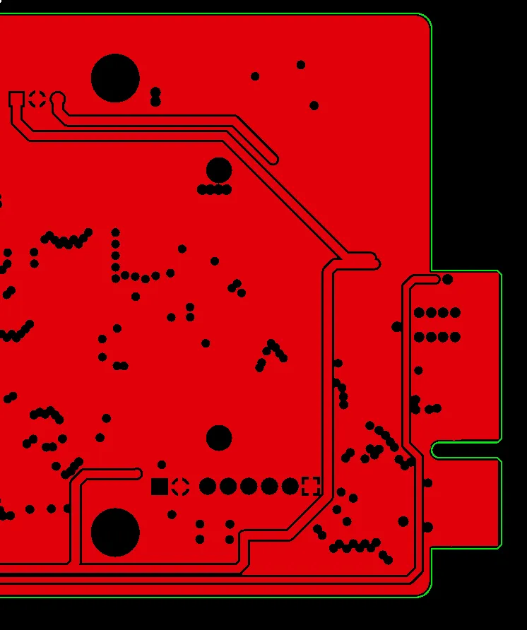
2.Gold Finger Area Thickness Issues
If the inner layer under a gold finger is too empty, lamination pressure causes local thickness variation. The gold finger may become thinner than expected, leading to poor connector contact.
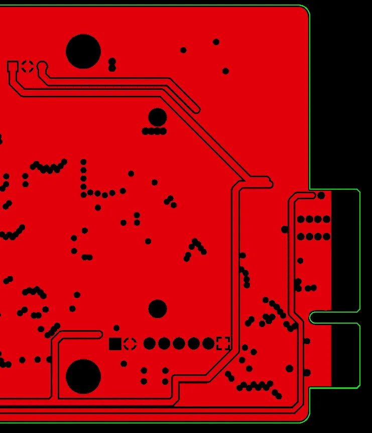
ALLPCB solution: Even if no electrical requirement exists, ALLPCB adds dummy copper pour in PCB gold finger areas to equalize lamination pressure. Using high Tg or low-flow resin further ensures uniform thickness.
4.Copper Pour Design Guidelines
- Avoid leaving large empty zones; always consider copper pour PCB design.
- Keep copper distribution uniform across layers to prevent warpage.
- Always add copper under gold fingers to ensure thickness consistency.
- If copper cannot be added, keep at least 8 mil spacing for 2oz copper designs.
5.Why Choose ALLPCB’s Copper Pour Solution?
Professional DFM Review
Upon receiving Gerber files, ALLPCB automatically checks for large empty zones. Our engineers provide tailored PCB copper pour balance strategies, especially for gold fingers, BGA zones, and differential lines.

Reliable Manufacturing Control
Advanced automated plating lines and real-time monitoring ensure consistent copper deposition, even in boards with complex copper distribution.

Problem-Specific Solutions
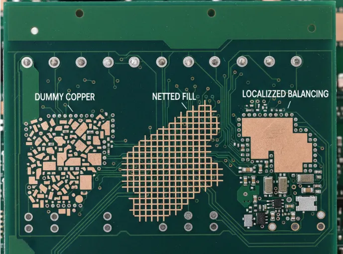
Instead of generic “fill copper everywhere,” ALLPCB offers case-specific compensation strategies: dummy copper, netted fill, or localized copper pouring methods.
Fast Delivery + Expert Support
ALLPCB guarantees fast delivery for every PCB order. Beyond speed, our expert support team provides reliable after-sales service, ensuring quick responses, problem-solving, and long-term partnership. With one-on-one engineer consultation, customers can resolve copper design questions quickly and get boards manufactured with confidence.

Conclusion
Less copper doesn’t always mean lower cost—it can lead to plating imbalance, warpage, and reliability risks that increase expenses in the long run. At ALLPCB, we deliver the real copper pour solution: optimized copper balance, advanced material options, and expert design support. With fast delivery and reliable after-sales service, we ensure your PCB not only saves cost but also achieves the highest performance and stability.
Know more information about copper pour, please click here: