ALLPCB


Overview
This article examines common GPU system architectures and their typical hardware components.
Examples discussed include an 8-node system with NVIDIA A100 GPUs and an 8-node system with NVIDIA A800 GPUs.
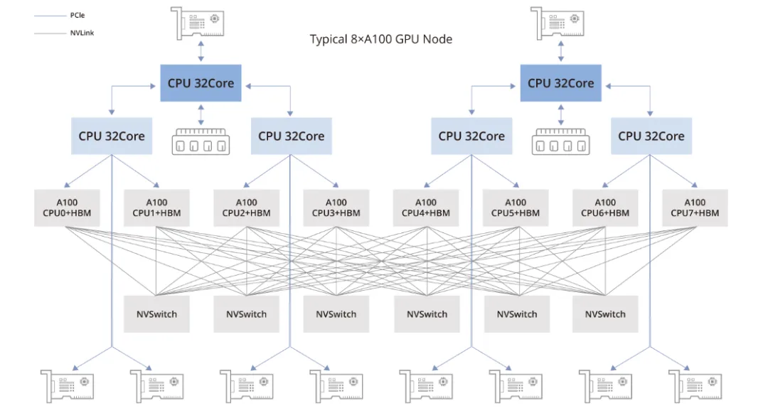
Typical A100 GPU Topology
In the A100 GPU topology shown below, the 8-GPU configuration includes the following components:
- Two CPU chips and their associated memory (NUMA architecture): Central processors handle general-purpose compute tasks.
- Two storage network interface cards (for accessing distributed storage with in-band management features): These NICs provide access to distributed storage resources.
- Four PCIe Gen4 switch chips: PCIe Gen4 is the fourth generation of the PCIe interface, offering higher data transfer rates.
- Six NVSwitch chips: NVSwitch enables very high-speed GPU-to-GPU communication, which is critical for large-scale deep learning nodes and parallel compute workloads.
- Eight GPUs: A100 GPUs serve as the primary parallel compute units, suitable for AI and deep learning workloads.
- Eight GPU-dedicated network interface cards: Each GPU is paired with a dedicated NIC to optimize inter-GPU communication and overall parallel processing performance.
The following image shows a more detailed topology for reference.
Storage Network Interface Cards
Storage NICs in GPU architectures connect to the CPU via the PCIe bus and facilitate communication with distributed storage systems. Their main roles include:
- Reading and writing distributed storage data: Efficient access to distributed datasets is critical for deep learning training, including frequent reads of training data and periodic writes of checkpoints.
- Node management tasks: Storage NICs often handle remote management tasks such as SSH access, system monitoring, and data collection for cluster maintenance.
Although the official recommendation is to use BF3 DPU, in practice alternative solutions can be used as long as bandwidth requirements are met. For cost efficiency, RoCE may be considered; for maximum performance, InfiniBand is typically preferred.
NVSwitch Network
In a fully connected network topology, each GPU is directly connected to every other GPU. Typically, the 8 GPUs are interconnected through six NVSwitch chips in a full-mesh configuration, commonly referred to as an NVSwitch architecture.
In a full-mesh configuration, the bandwidth of each link depends on the per-NVLink channel bandwidth, expressed as n * bw-per-nvlink-lane. For A100 GPUs using NVLink3 with 50GB/s per channel, each link in the full-mesh provides a total bandwidth of 12 * 50GB/s = 600GB/s bidirectional, which equates to 300GB/s unidirectional.
By contrast, A800 GPUs reduce the number of NVLink channels from 12 to 8. In a full-mesh configuration, each link provides 8 * 50GB/s = 400GB/s bidirectional, or 200GB/s unidirectional.
The following is an example nvidia-smi topology diagram for a device built from 8 A800 GPUs.
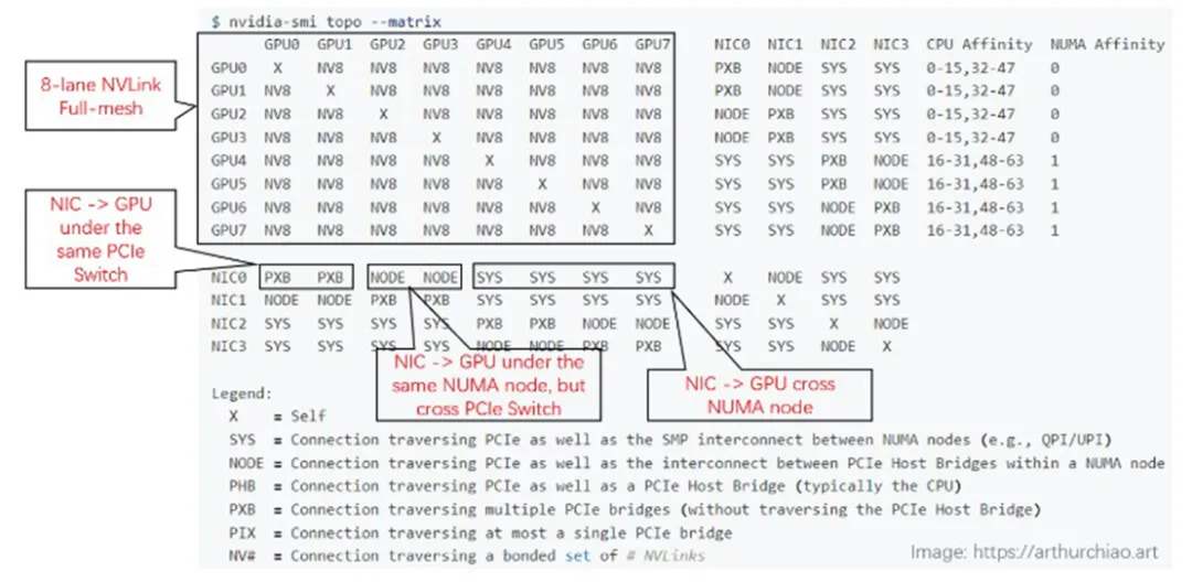
Notes on topology labeling:
- GPU-to-GPU connections (upper-left area): All connections are labeled NV8, indicating eight NVLink connections.
- NIC connections within the same CPU chip: Labeled NODE, indicating no NUMA crossing but traversal through PCIe switch chips is required.
- NIC connections between different CPU chips: Labeled SYS, indicating NUMA crossing is required.
- GPU-to-NIC connections within the same CPU chip and the same PCIe switch: Labeled NODE, indicating only PCIe switch traversal is needed.
- GPU-to-NIC connections within the same CPU chip but different PCIe switches: Labeled NNODE, indicating traversal of both PCIe switches and the PCIe host bridge chip.
- GPU-to-NIC connections between different CPU chips: Labeled SYS, indicating NUMA crossing, PCIe switch traversal, and the longest path.
GPU Node Interconnect Architecture
The diagram below illustrates the interconnect architecture between GPU nodes.
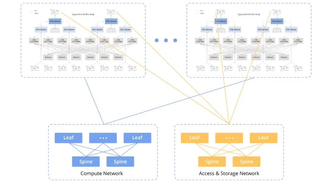
Compute Network
The compute network connects GPU nodes to support coordinated parallel compute tasks, including data transfers between GPUs, sharing of intermediate results, and orchestration of large-scale parallel workloads.
Storage Network
The storage network connects GPU nodes to storage systems and supports large-scale data read and write operations, such as loading data into GPU memory and writing back computation results.
To meet AI application performance requirements, RDMA technologies are important on both the compute and storage networks. Choosing between RoCEv2 and InfiniBand involves trade-offs between cost and performance, with each option optimized for specific use cases and budgets.
Public cloud providers often use RoCEv2 networks in their configurations. For example, some configurations include 8 GPU instances, each with 8 x 100Gbps. Compared with other options, RoCEv2 can be more cost effective when it meets performance requirements.
Bandwidth Bottlenecks in Data Links
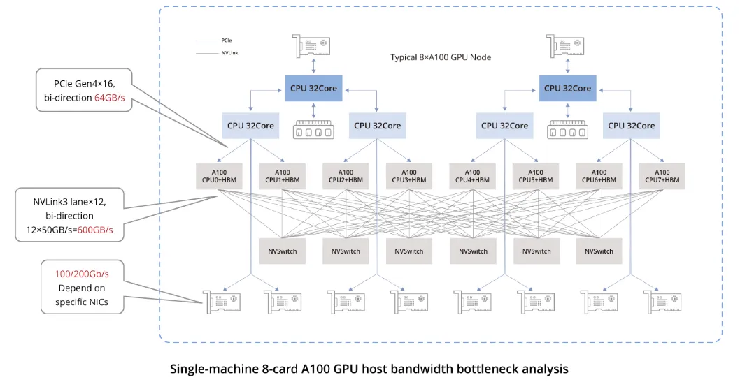
The chart highlights bandwidth specifications for key connections:
- GPU-to-GPU communication within the same host: Via NVLink, with 600GB/s bidirectional and 300GB/s unidirectional.
- GPU-to-NIC communication within the same host: Via PCIe Gen4 switches, typically 64GB/s bidirectional and 32GB/s unidirectional.
- GPU-to-GPU communication between different hosts: Relies on NICs, and bandwidth depends on the specific NIC used. Currently in the Chinese market, common NICs used with A100/A800 models offer a typical unidirectional bandwidth of 100Gbps (12.5GB/s). Therefore, inter-host GPU communication performance is significantly lower than intra-host communication.
- 200Gbps corresponds to 25GB/s, which approaches PCIe Gen4 unidirectional bandwidth. 400Gbps corresponds to 50GB/s, which exceeds PCIe Gen4 unidirectional bandwidth.
Consequently, using 400Gbps NICs in such configurations does not provide a significant advantage unless the system also provides PCIe Gen5-level performance to fully utilize that bandwidth.
8x NVIDIA H100 / 8x NVIDIA H800 Hosts
H100 Host Hardware Topology
The overall hardware architecture of an H100 host is similar to the A100 eight-GPU system but differs in the number of NVSwitch chips and NVLink bandwidth upgrades.
Each H100 host uses four NVSwitch chips, two fewer than the A100 configuration.
The H100 GPU is manufactured on a 4 nm process. The bottom row includes 18 Gen4 NVLink connections, providing 18 channels * 25GB/s = 450GB/s per direction, or 900GB/s total bidirectional bandwidth.
H100 GPU Chip
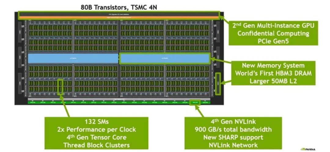
The H100 chip is built on an advanced 4 nm process. The bottom row contains 18 Gen4 NVLink links, delivering a total bidirectional bandwidth of 18 * 25GB/s = 900GB/s.
The central blue area represents the L2 cache, a high-speed buffer for temporary data. High-bandwidth memory (HBM) modules are integrated on the left and right sides of the chip to store data required for graphics processing and accelerator workloads.