ALLPCB


Overview
According to TrendForce data, about 130,000 AI servers were shipped, representing roughly 1% of global server shipments. Microsoft, Meta, Baidu, and ByteDance increased orders in 2023 as they launched services based on generative AI, and AI server shipments were expected to grow by 15.4% year over year in 2023. With continued demand driven by large models such as ChatGPT, AI server shipments are projected to grow at a 12.2% compound annual growth rate from 2023 to 2027.
DGX H100 Architecture
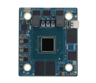
The DGX H100, launched in 2022, is NVIDIA's latest DGX system iteration and a foundation for DGX SuperPOD deployments. A DGX server is equipped with eight H100 GPUs, featuring 640 billion transistors. Under the new FP8 precision, AI performance is 6 times higher than the previous generation, and the system can provide 900 GB/s of bandwidth.
Inside a DGX H100 server, blue modules are IP network cards that function both as NICs and as PCIe switch expansion elements, bridging the CPU and GPUs (H100). These modules implement the PCIe 5.0 standard. The CX7 is implemented as two cards inserted into the server, with four CX7 chips per card and two external 800G OSFP optical module ports per card.
GPU-to-GPU interconnect is handled mainly by NVSwitch chips. Each GPU in a DGX H100 exposes 18 NVLink links, with a single-link bidirectional bandwidth of 50 GB/s, totaling 18 × 50 GB/s = 900 GB/s bidirectional bandwidth. This bandwidth is distributed across four onboard NVSwitch chips, so each NVSwitch corresponds to 4–5 OSFP optical modules (18 modules in total). Each OSFP optical module uses 8 optical lanes at 100 Gbps per lane, producing an 800 Gbps aggregate per module for high-speed data transmission.
1. CPU, GPU and Component Interconnect: PCIe Switch and Retimers
A PCIe switch connects PCIe devices and enables more devices to share a single PCIe root port by expanding or aggregating endpoints. PCIe is an end-to-end link protocol, so switches are required to address limitations in available lanes or ports. PCIe switches are widely used in storage and increasingly in server platforms to improve data throughput.
PCIe bus technology has evolved through multiple generations, and PCIe switch performance rises with each generation. PCIe evolved from the older parallel PCI bus into a high-speed serial interface. In 2001 Intel proposed a third-generation I/O technology called "3GIO", which was renamed "PCI Express" by the PCI Special Interest Group (PCI-SIG) in 2002. PCIe 1.0 was released in 2003 with 2.5 GT/s per lane (equivalent to 250 MB/s per lane). PCIe 2.0 doubled that to 5 GT/s per lane. PCI-SIG released the PCIe 6.0 specification in 2022, increasing per-lane signaling to 64 GT/s.
As PCIe usage in servers grows, demand for PCIe switches has expanded. According to QYResearch, global PCIe chip market revenue reached approximately $790 million in 2021 and is forecast to reach $1.8 billion by 2028, a CAGR of 11.9%.
The Chinese market represents the largest demand center for PCIe switches. With increasing requirements for large-scale data storage and transfer in big data, cloud computing, and AI, there is strong demand for high-speed interconnect solutions to handle massive data flows. PCIe switches are positioned to address those needs in the Chinese market.
In AI servers, a Retimer chip is typically required between CPU and GPU to ensure signal integrity. Many AI servers deploy multiple Retimers; for example, Astera Labs configures four Retimers in some AI accelerator designs.
The PCIe Retimer market is competitive. Currently, PuRui-KY, Astera Labs, and Lanqi Technology are notable players in this segment. Lanqi Technology entered the PCIe market early and is the only mainland China supplier that has shipped mass-producible PCIe 4.0 Retimers, with PCIe 5.0 Retimer development reportedly progressing.
Other semiconductor vendors such as Renesas, Texas Instruments, and Microchip Technology have also developed or announced PCIe Retimer products. For example, Renesas offers PCIe 3.0 Retimers including models 89HT0816AP and 89HT0832P; Texas Instruments offers the DS160PT801, a 16 Gbps 8-channel PCIe 4.0 Retimer; Microchip released the XpressConnect series in November 2020, supporting PCIe 5.0 at 32 GT/s.
2. GPU-to-GPU Interconnect: NVLink and NVSwitch
Major chip vendors are focusing on high-speed interconnect technologies. Beyond NVIDIA's NVLink, AMD's Infinity Fabric and Intel's CXL (Compute Express Link) also provide internal high-speed server interconnect solutions.
NVLink has driven advances in high-bandwidth interconnects. Developed by NVIDIA, NVLink accelerates data transfer between CPU and GPU and between GPUs to improve system performance. From 2016 through 2022, NVLink evolved to its fourth generation.
The first-generation NVLink, introduced with the Pascal GP100 GPU in 2016, used NVHS signaling and transmitted differential NRZ-encoded electrical signals between GPUs and between CPU and GPU. A single first-generation NVLink link provided 40 GB/s bidirectional bandwidth, and a GPU could support 4 links for a total of 160 GB/s bidirectional bandwidth per chip.
Subsequent NVLink generations increased aggregate bandwidth. The second-generation NVLink (Volta, 2017) provided 50 GB/s per link and up to 6 links per chip for 300 GB/s aggregate. The third generation (Ampere, 2020) maintained 50 GB/s per link and increased to 12 links per chip for 600 GB/s aggregate. The fourth generation (Hopper, 2022) moved to PAM4 signaling while keeping 50 GB/s per link, supporting up to 18 links per chip for 900 GB/s aggregate.
NVIDIA released the first NVSwitch in 2018 to increase internal bandwidth, reduce latency, and enable multi-GPU communication. The first NVSwitch was manufactured on TSMC 12 nm FinFET and provided 18 NVLink 2.0 ports; a single server could use 12 NVSwitch devices to interconnect 16 V100 GPUs at NVLink speeds.
NVSwitch has evolved to a third generation. The third-generation NVSwitch is built on TSMC 4N process and offers 64 NVLink 4.0 ports per chip, enabling GPU-to-GPU communication at up to 900 GB/s. GPUs interconnected via NVLink Switch can be used as a single high-performance accelerator for deep learning workloads.
3. CPU-to-DRAM High-Speed Interconnect and Memory Interface Chips
Server memory modules are typically RDIMM and LRDIMM. Compared with other module types, server memory prioritizes stability, error correction, and low power. The memory interface chip is the core logic device on a server memory module and is the necessary path for the CPU to access memory data. Its principal functions are to improve memory access speed and stability and to meet server CPU demands for higher performance and larger capacity.
From DDR4 to DDR5, interface chip speeds have kept increasing. DDR4 became mainstream beginning in 2016. JEDEC refined DDR4 interface specifications across subgenerations from Gen1.0, Gen1.5, Gen2.0 to Gen2plus, with Gen2plus supporting up to 3200 MT/s. JEDEC has defined DDR5 specifications and DDR5 technology is succeeding DDR4.
DDR5 memory interface chips are planned across three subgenerations supporting 4800 MT/s, 5600 MT/s, and 6400 MT/s, with industry expectations for one or two additional subgenerations in the future.
Memory interface chips are classified by function into the register clock driver (RCD) and the data buffer (DB). The RCD buffers addresses, commands, and control signals from the memory controller. The DB buffers data signals from the memory controller or memory die.
The DDR5 upgrade creates opportunities for memory interface chips and module companion chips. The global memory interface chip market was approximately $280 million in 2016 and rose to about $570 million in 2018, a three-year CAGR of 40%. DDR5’s higher speeds and more complex designs lead to higher initial unit prices for first-generation DDR5 interface chips compared with DDR4. As DDR5 penetration increases in servers and PCs, the DDR5-related memory interface chip market is expected to grow rapidly.
High barriers exist in the memory interface chip industry, and a three-player market structure has formed. Memory interface chips are technology-intensive and require comprehensive validation by CPU, memory, and OEM vendors before mass deployment, making it difficult for new entrants. From more than ten suppliers in the DDR2 era, the market consolidated to three suppliers by DDR4. For DDR5 first-generation mass-production products, only three global suppliers are available: Lanqi Technology, Renesas Electronics (IDT), and Rambus.