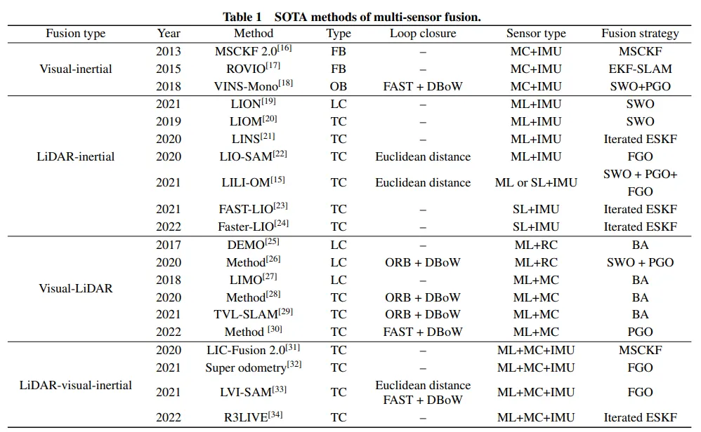
ALLPCB


Overview
With the advent of CMOS 2.0, chip design is approaching a significant transition. CMOS has been the silicon logic technology behind smaller transistors and faster computers for decades. While the basic complementary pair of transistors used to reduce circuit power remains, the way processors and other complex CMOS chips are manufactured is changing. Julien Ryckaert, Imec's vice president of logic technology, outlined this evolution to IEEE Spectrum.
Why is CMOS entering a new phase?
Ryckaert explains that CMOS was the technology choice for building microprocessors in the 1960s. Shrinking transistors and interconnects improved performance for many decades, but that trend is becoming increasingly difficult to sustain. Designers have been integrating more and more functions onto the same silicon die—CPUs, GPUs and other system-on-chip (SoC) blocks—because moving data on a die is far more efficient than moving it between chips. Historically, device and interconnect scaling enabled this integration, but now simply shrinking devices and interconnects is no longer sufficient. Different functions such as SRAM and logic no longer scale equally well.
Challenges of modern CMOS scaling
Advances in semiconductor technology have introduced complex challenges for continued CMOS scaling. Making transistors smaller to improve performance encounters limits from power consumption, heat dissipation and quantum effects. Balancing these factors is critical to sustaining innovation in electronic devices.
Short-channel effects (SCE)
Short-channel effects occur when device dimensions reach the micron and submicron regimes, affecting MOSFET behavior. As gate length decreases, gate control over the channel weakens and drain-induced fields increase. This leads to higher leakage currents, reduced carrier mobility and degraded threshold-voltage control. Historically, mitigation focused on thinning the gate oxide and engineering source/drain/channel doping profiles. The industry also adopted new materials and device architectures—strained channels, high-k metal gates (HKMG), silicon-on-insulator (SOI) and FinFETs—to suppress SCE and other adverse effects.
Limits of traditional scaling
Continued scaling of CMOS has encountered limits due to the diminishing returns of traditional approaches. Recent roadmaps indicate that for low-power and high-performance applications, physical gate length scaling below roughly 14 nm and 12 nm, respectively, will be increasingly difficult to sustain. This presents significant obstacles for further density and performance improvements.
Device electrostatics and variability
Improving device electrostatics and addressing variability in ultra-scaled MOSFETs has become central to modern scaling efforts. Device electrostatics quantify a FET's scalability through the natural length parameter, lambda, which captures how potential changes from source or drain penetrate the channel. Effective modulation of the channel potential is essential for controlling mobile charge; solving these electrostatic challenges is key to scaling.
What is the proposed solution?
Ryckaert argues that Moore's law is fundamentally about packing more functionality per unit area, not merely making smaller transistors and interconnects. One emerging approach is to split certain functions, such as logic and SRAM, into separate small dies built with the most appropriate technologies for each function, and then re-integrate them using advanced 3D packaging. This disaggregation allows connecting functions built on different substrates with communication efficiency comparable to that of functions on the same substrate. This approach is referred to as functional decomposition or system-level co-optimization.
What defines CMOS 2.0?
CMOS 2.0 extends this idea with finer-grained functional decomposition and greater die stacking. An early sign of CMOS 2.0 is the move to backside power networks. Currently, all interconnects on a chip—both those that carry data and those that deliver power—are on the front side above the transistors. These interconnect types have different requirements, but until now have shared the same interconnect stack with compromises. Backside power delivery moves the power-delivery interconnects under the silicon, effectively turning the chip into an active transistor layer sandwiched between two interconnect stacks, each optimized for different functions.
Do transistors and interconnects still need to shrink?
Yes. Even with stacked dies, some layers will require higher transistor density, so scaling is still needed at least for those layers. However, by removing many of the previous constraints, each layer can scale using the technology best suited to its function.
Potential applications
CMOS 2.0 could impact many sectors:
- AI: Neuromorphic and specialized chips could accelerate training and inference for complex algorithms.
- IoT: Smaller, more energy-efficient devices could benefit from die-level optimization.
- High-performance computing: Advanced chip architectures enabled by stacking could unlock new compute capability.
- Consumer electronics: Denser and more efficient chips could lead to more capable smartphones, laptops and other devices.
Architecture and cache hierarchy
Imec envisions full 3D chip design. For example, AMD's second-generation 3D V-Cache stacks L3 memory on top of the processor die to increase capacity; Imec imagines entire cache hierarchies on their own layers, with L1, L2 and L3 vertically stacked on top of the transistor layer that forms the processing cores. Each cache level could use transistors and process nodes optimized for that task. As SRAM scaling slows, moving caches to lower-density nodes via 3D stacking could reduce cost per MB and enable much larger caches than previously practical. Properly designed 3D stacks can also help mitigate latency issues associated with larger caches.
Conclusion
CMOS 2.0 represents an evolution in chip design that combines new materials, device structures and design paradigms to address limits of current scaling. Its full impact depends on continued research and development across the semiconductor ecosystem. Key questions remain about EDA tool development, partitioning costs and complexity, and thermal management of 3D platforms. The transition is not simply a continuation of past scaling trends but a structural shift in how functions are partitioned and integrated at the die and package level.