ALLPCB


Overview
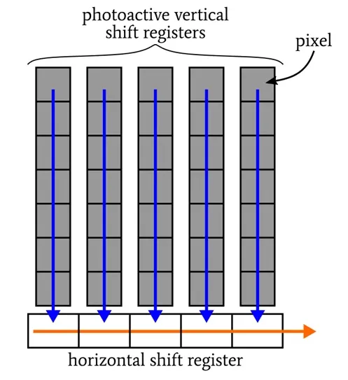
The semiconductor region in a CCD can act both as a photosensitive element and as a charge-transfer device. In a full-frame (FF) CCD, pixel sites respond to incident photons during the integration period and accumulate charge. After integration, the charge packets are shifted vertically through the pixel sites into a horizontal shift register for readout.
Pixel readout is achieved by applying carefully timed clock signals that sequentially create potential wells and barriers in the device's charge-transfer structure. In a full-frame CCD, these control voltages must be applied to areas that also serve as photodetectors, so the gate electrodes are commonly made from transparent polysilicon.
Full-frame CCDs are relatively simple to manufacture and allow the entire CCD surface to be photosensitive. That maximizes the number of pixels per unit silicon area and increases the fraction of incident photons each pixel can convert into electrons. A major limitation, however, is the need for a mechanical shutter (or a synchronized short-duration light source). The photosensitive area does not stop integrating simply because a readout begins; without a shutter to block incident light after exposure, charges generated during readout can corrupt the image.
Frame-Transfer (FT) CCD
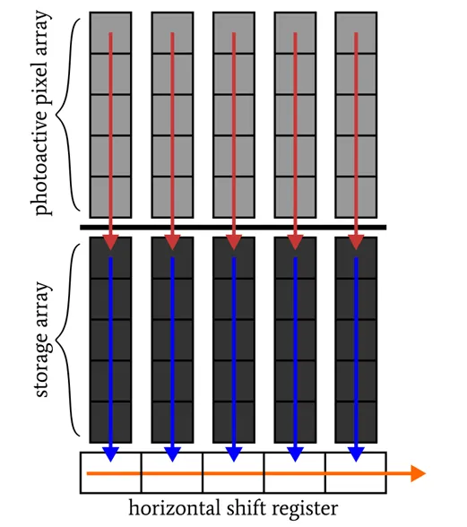
Frame-transfer CCDs retain many of the advantages of full-frame CCDs while largely removing the need for a mechanical shutter. The sensor is split into two equal parts: an active imaging array and a light-shielded storage array. After exposure, all pixel charge packets are rapidly transferred to the storage array and then read out from there. While the storage area is being read, the active pixels can immediately begin integrating the next frame, enabling higher frame rates than full-frame CCDs.
The transfer from the imaging array to the storage area is very fast but not instantaneous, so some vertical smear can occur from photons arriving during the transfer. Frame-transfer CCDs also tend to be larger and more costly per effective pixel because half the silicon area is used for storage rather than light collection.
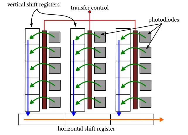
Interline-Transfer (IT) CCD
Interline-transfer CCDs address smear by providing a storage and transfer region adjacent to each photosensitive site. After exposure, each charge packet is transferred simultaneously into a non-photosensitive vertical shift register. This enables an effective electronic shutter with significantly reduced vertical smear while retaining the ability to integrate during readout for high frame rates.
Interline-transfer CCDs eliminate the large storage area used in frame-transfer designs, but introduce a different drawback: reduced fill factor. Each pixel now comprises a photosensitive diode and a portion of the vertical transfer register, so part of the pixel area is not light-sensitive and fewer electrons are generated for the same incident light. Using microlenses to concentrate incoming light onto the photosensitive region can substantially mitigate this sensitivity loss, although microlenses bring their own manufacturing challenges.

Conclusion
Each CCD architecture involves trade-offs. Full-frame CCDs maximize photosensitive area and are suitable when high frame rates are not required and a mechanical shutter or strobe can be used. Frame-transfer and interline-transfer CCDs provide electronic shuttering and higher effective frame rates; they are widely used where those capabilities are necessary despite the associated area, cost, or fill-factor compromises.