ALLPCB


Overview
CCD voltages are nonstandard. Clock high levels are often higher than the voltages used for CMOS logic, and low levels frequently extend below ground.
Below are representative examples from several CCD datasheets.
Examples from Datasheets
On Semiconductor KAI-1020: This is an interline-transfer device with 1000 × 1000 active pixels. The control voltage range is -9 V to +15 V. Control signals applied to the chip use 5 V logic; internal drivers translate the logic signals to the voltage levels required by the charge-transfer gates.
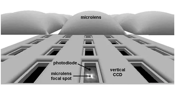
The KAI-1020 datasheet includes a smooth 3D rendering of an interline-transfer CCD.
Sony ICX059CL: This is a 752 × 582 pixel interline-transfer CCD for monochrome cameras. If the datasheet is interpreted correctly, it uses +15 V to transfer charge packets from the photodiodes to the vertical shift register, -8.5 V to 0 V for vertical transfer clocks, and 0 V to +5 V for horizontal transfer. The diagram below shows the overall architecture.
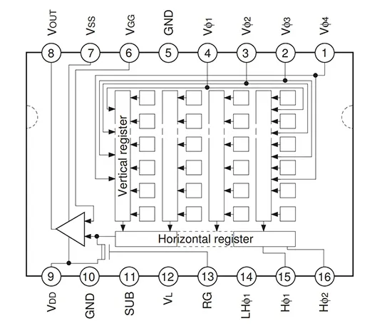
Diagram from the ICX059CL datasheet.
Texas Instruments TC281: This 1000 × 1000 image sensor uses a frame-transfer architecture. Most clocks have a low level of -10 V and a high level of +2 V.
The area marked with an × symbol is the photosensitive pixel array; the lower section is the storage array.
Readout Clock Configurations
At the semiconductor level, charge packets are moved from pixels to the output terminal by applying sequences of voltages that create potential wells and barriers. There are several methods to produce the required potential changes.
Four-Phase Clocking
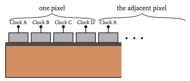
The direct method uses four clock phases. Each pixel has four gates, so four separate clock signals are applied to the four parts of a pixel to move a charge packet to the adjacent pixel.
For interline-transfer CCDs, the term shift-register section is often used instead of pixel, since charge packets do not move through photosensitive regions in an interline architecture.
The sequence starts at phase 1. Clocks A and B are high, clocks C and D are low. Here, high means a higher voltage that creates a potential well that attracts electrons, while low produces a barrier that blocks electrons.
Refer to the diagram below while following the next three phases.
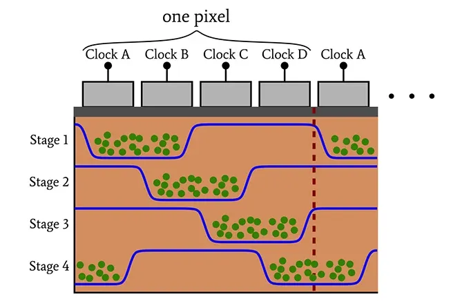
In phase 1, charge accumulates in the potential wells under gates A and B and is blocked by barriers under gates C and D.
In phase 2, clock A goes low and clock C goes high; clocks B and D remain unchanged. This shifts the electrons one step to the right because wells now exist under gates B and C while barriers exist under gates A and D.
In phase 3, clock B goes low and clock D goes high. Electrons are pushed another step to the right as the wells move under gates C and D.
In phase 4, clock A goes high and clock C goes low. A potential well now extends from gate D of one pixel to gate A of the next pixel.
Phase 5 is the same as phase 1. The charge has fully transferred to the adjacent pixel and the cycle continues.
Three-Phase, Two-Phase, and Single-Phase Clocks
A drawback of four-phase control is that sensor resolution is limited by having four gates per pixel. Reducing the number of clocks allows smaller pixel sizes and higher pixel density, but the applied voltages become more complex.
Alternatives to four-phase control include three-phase, pseudo-two-phase, true two-phase, and virtual-phase (single-clock) schemes. For example, the KAI-1020 uses two-phase clocking, the ICX059CL uses four-phase clocking, and the TC281 uses a proprietary virtual-phase scheme described by TI.