 ALLPCB


CEM-1 PCB material offers electronics designers a practical option when balancing performance requirements with environmental considerations. This composite substrate combines epoxy resin with cellulose-based reinforcement, typically paper or a blend that includes woven glass elements in limited quantities. Engineers often select it for single-sided or simple double-sided boards where cost and material efficiency matter. Its lower glass fiber content compared with some other laminates can influence both manufacturing energy use and end-of-life handling. Industry professionals continue to evaluate such materials as part of broader efforts toward greener electronics production.
What Is CEM-1 PCB and Why It Matters
CEM-1 stands for composite epoxy material type 1, a substrate developed for applications that do not require the high mechanical strength or thermal performance of glass-epoxy laminates. The reinforcement consists primarily of cellulose fibers or paper impregnated with epoxy resin, sometimes incorporating a thin layer of woven glass on the surface. This construction yields a material suitable for consumer electronics, automotive controls, and industrial devices operating at moderate temperatures and frequencies.
The environmental profile of CEM-1 draws attention because reduced glass content can lower the energy required during laminate production and simplify certain recycling streams. Designers working on green electronics projects examine CEM-1 PCB environmental impact alongside factors such as halogen-free formulations and compliance with material restrictions. Sustainable PCB manufacturing practices increasingly consider substrate choice as one element in reducing overall product footprint. Procurement teams and engineers therefore review CEM-1 specifications when projects emphasize resource efficiency without compromising basic electrical performance.
Technical Principles of CEM-1 Construction and Performance
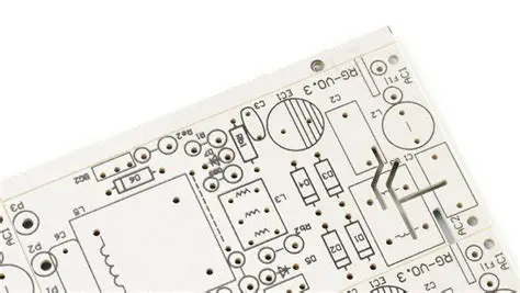
The manufacturing process for CEM-1 begins with impregnation of cellulose sheets or paper with epoxy resin, followed by drying and pressing under controlled heat and pressure. A surface layer of woven glass fabric may be added to improve copper adhesion and dimensional stability during etching and assembly. This layered structure results in a substrate with adequate rigidity for many single-sided circuits while maintaining lower density than fully glass-reinforced alternatives.
Electrical properties remain suitable for low- to medium-speed digital and analog circuits, with dielectric constants that support acceptable signal integrity in non-critical paths. Thermal conductivity stays modest, so designers must account for heat dissipation through other means such as copper planes or external heatsinks. Moisture absorption tends to be higher than in glass-epoxy materials, requiring careful attention to storage and baking procedures before soldering.
Industry standards such as IPC-6012E guide qualification testing for rigid printed boards, ensuring that CEM-1 constructions meet defined electrical and mechanical criteria. Engineers apply these requirements during material selection to confirm suitability for the intended operating environment.
Design and Manufacturing Practices for Sustainable Outcomes
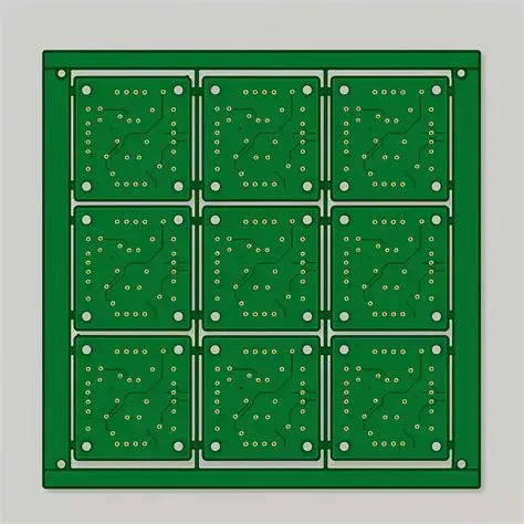
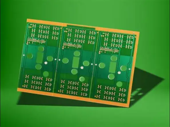
Engineers optimize CEM-1 PCB designs by minimizing copper usage, selecting appropriate trace widths, and avoiding unnecessary layers that increase material consumption. Panelization strategies that maximize board yield per sheet further reduce waste during fabrication. When specifying surface finishes, choices compatible with lead-free processes align with broader environmental goals without altering the substrate itself.
Sustainable PCB manufacturing benefits from consistent process controls that limit scrap and energy consumption. Fabricators monitor press cycles and curing parameters to achieve required properties with minimal excess resin or reinforcement. After assembly, boards using CEM-1 can enter standard electronics recycling streams where metals are recovered and the remaining laminate undergoes separation or energy recovery depending on local facilities.
CEM-1 PCB recycling potential improves when designers avoid mixing multiple substrate types within the same product family, simplifying downstream sorting. Quality control procedures outlined in standards such as IPC-A-600K help maintain acceptable board quality, reducing the likelihood of early failures that would increase overall environmental burden through replacements.
Best Practices for Integration in Green Electronics Projects
Procurement and design teams evaluate CEM-1 when the application allows single- or double-sided construction and operating temperatures remain within the material's typical limits. Early collaboration between electrical and mechanical engineers ensures thermal and mechanical stresses stay manageable without additional reinforcements. Documentation of material declarations supports compliance verification and future recycling planning.
Testing protocols include thermal cycling, humidity exposure, and electrical performance checks aligned with relevant IPC and JEDEC standards. These steps confirm long-term reliability while documenting the environmental attributes of the chosen substrate. When projects target reduced environmental impact, CEM-1 serves as one option among several, selected through comparative analysis of performance data and lifecycle considerations.
Conclusion
CEM-1 PCB material provides engineers with a technically viable substrate that supports efforts to lower the environmental impact of electronic products. Its cellulose-reinforced construction offers material efficiency advantages in appropriate applications, while established industry standards ensure consistent quality and performance. Thoughtful design, controlled manufacturing, and attention to end-of-life handling allow this material to contribute to sustainable PCB manufacturing goals. Continued evaluation of substrate options remains essential as regulations and market expectations for green electronics evolve.
FAQs
Q1: What factors influence the CEM-1 PCB environmental impact compared with other substrates?
A1: Material composition plays a central role, with lower glass fiber content potentially reducing production energy and simplifying certain recycling processes. Engineers assess the full product lifecycle, including manufacturing waste, assembly compatibility, and end-of-life recovery, when comparing CEM-1 with alternatives. Compliance with material standards helps maintain performance while supporting environmental objectives.
Q2: How does sustainable PCB manufacturing incorporate CEM-1 materials?
A2: Sustainable practices focus on efficient panel utilization, controlled processing parameters, and selection of compatible finishes that minimize waste. CEM-1 integrates into these workflows when design requirements align with its mechanical and thermal characteristics. Documentation of processes supports traceability and continuous improvement in resource use.
Q3: What considerations apply to CEM-1 PCB recycling at end of life?
A3: Recycling streams for CEM-1 boards follow established electronics recovery methods that separate metals first, after which the remaining laminate may undergo further processing or energy recovery. Consistent use of a single substrate type within a product family aids sorting efficiency. Local regulations and facility capabilities ultimately determine the most effective recovery route.
Q4: Can CEM-1 contribute to green electronics design goals?
A4: CEM-1 supports green electronics initiatives when selected for applications matching its performance envelope and when paired with responsible design and manufacturing practices. Engineers review environmental attributes alongside electrical and reliability requirements to determine suitability. Ongoing material evaluation helps align product development with sustainability targets.
References
IPC-6012E — Qualification and Performance Specification for Rigid Printed Boards. IPC, 2017
IPC-A-600K — Acceptability of Printed Boards. IPC, 2020
JEDEC J-STD-020E — Moisture/Reflow Sensitivity Classification. JEDEC, 2014





