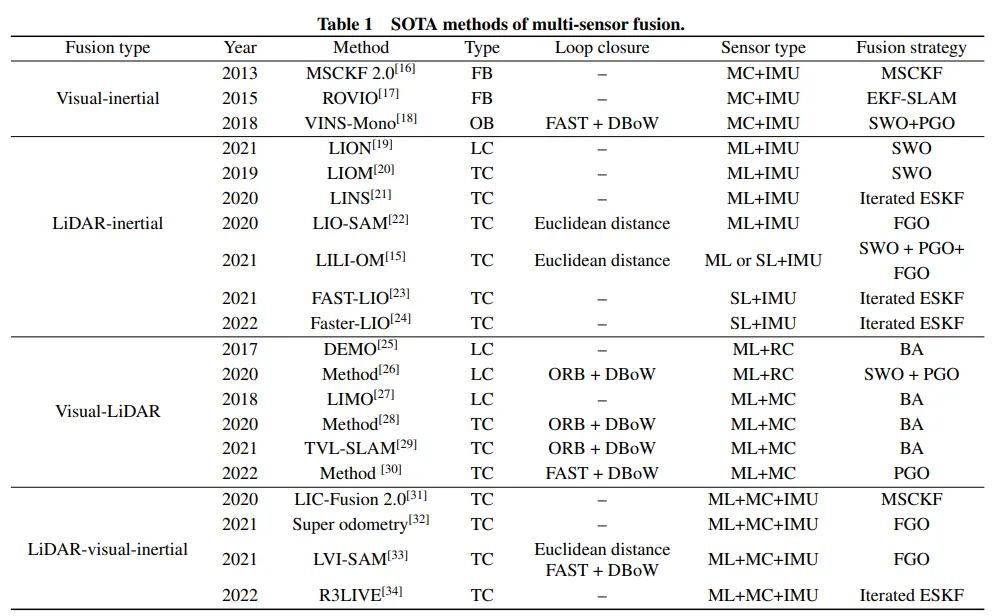
ALLPCB


Overview
The photosensitive element used for imaging in cameras is called an image sensor or imager. The two widely used image sensor types today are CCD and CMOS image sensors (CIS).
Introduction
CCD technology has been widely used in digital cameras, but CCDs consume significant power and require many supporting chips. CMOS image sensors were developed to address these issues. Each pixel in a CMOS sensor can perform its own charge-to-voltage conversion, reducing power consumption and the need for external support circuitry. CMOS image sensors are manufactured using materials and processes similar to those used for microprocessors and memory chips, which makes production easier and more cost-effective, so they are widely used in mobile phones and other portable devices. This article focuses on the principles and details of CMOS image sensors.
1. CMOS Sensor Principles
CMOS stands for complementary metal-oxide semiconductor, a mainstream semiconductor process known for low power consumption and high speed, and widely used for CPUs, memory, and digital logic chips. Image sensors designed with CMOS processes are called CMOS image sensors (CIS) and share over 90% similarity with general semiconductor processes, especially memory processes.
CMOS image sensors use CMOS switches to select signals from individual photodiodes. Each pixel consists of a photodiode and a CMOS switch. When a row is selected by the row driver, the CMOS switches for that row turn on while switches for other rows remain off. The photoelectric signals from that row are transferred to the column multiplexer. The column multiplexer, implemented with a series of CMOS switches, sequentially connects that row's signals to the output, completing the sequential readout of a column of pixels.
2. CCD Image Sensors
A CCD device is essentially an analog shift register. Under clock control, signal charge is transferred from one potential well to another, enabling analog signal shifting. CCD image sensors use this charge-transfer function for scanning. Here is a schematic of CCD operation: signal multiplexing is implemented by vertical-transfer CCDs and horizontal-transfer CCDs. In practical CCD sensors, photoconversion devices are integrated with the vertical CCDs. The vertical CCDs move each row's photodiode signals sequentially to the horizontal CCDs, which then shift that row's signals to the output. Repeating this process produces a frame of image signals.
3. Comparison Between CCD and CMOS Image Sensors
A CCD typically uses a single charge-to-voltage converter. During readout, accumulated charge in each pixel must be shifted row by row under control of row voltages until it reaches the row buffer associated with the array, and then shifted column by column to the converter at the array output. One major advantage of CCDs is that all pixels share the same charge-to-voltage converter, producing excellent pixel uniformity. In contrast, CMOS sensors assign a dedicated charge-to-voltage converter to each pixel, which makes uniformity harder to control. When pixel counts exceed around 2 megapixels, sharing a single converter can limit readout speed, so multi-tap designs (two or four arrays with dedicated row buffers and converters) are used to speed up readout by multiples.
4. CMOS Sensor Pixel Structures
Passive Pixel
The simplest pixel structure consists of a PN junction as the photosensitive element and a reset transistor (RS) as a switch, as shown in Figure 1.
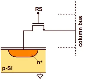
Figure 1: Single PN-junction passive pixel structure
Operation of a passive pixel:
Before exposure, the pixel's row select address is asserted, enabling RS and connecting the PN junction to the column bus. The column selector is also driven high, applying a reverse bias (e.g., 3.3 V) across the PN junction. After a short delay for charge equilibrium, the reset completes and RS is released to isolate the PN junction from the column bus.
During exposure, photons absorbed in the silicon generate electron-hole pairs. Under the PN junction electric field, electrons flow toward the n+ side and holes flow to the p-substrate, reducing the reverse bias across the PN junction.
After exposure, RS is enabled again and the readout circuit measures the PN junction voltage. The difference from the original reverse bias is proportional to the number of incident photons.
After reading the signal, the PN junction is reset again to prepare for the next exposure.
When RS is enabled and the column selector is high, the PN junction capacitance is effectively charged. The resulting voltage has randomness: physical variations in PN junction capacitance across pixels cause fixed pattern noise (FPN), and thermal/shot variations give rise to kTC noise. kTC noise depends on junction structure, temperature, and capacitance.
Active Pixel
Most modern CMOS sensors use active pixel structures. The 3T active pixel structure contains a photodiode and three transistors per pixel: a reset transistor (RST), a row select transistor (RS), and a source follower amplifier (SF).
Active pixel operation:
- Reset: RST is enabled to apply reverse bias to the photodiode, then RST is released.
- Exposure: same principle as passive pixels.
- Readout: after exposure, RS is activated and the photodiode signal is amplified by SF and read out.
- Cycle: after readout the pixel is reset and the cycle repeats.
PN-junction-based active pixels became popular in the mid-1990s and addressed many noise issues, but kTC noise introduced by the PN junction reset remained a problem.
Pinned Photodiode (PPD)
The introduction of the pinned photodiode (PPD) marked a major improvement in CMOS performance. PPD enables correlated double sampling (CDS), eliminating reset-induced kTC noise, amplifier 1/f noise, and offset noise, as shown in Figure 2.
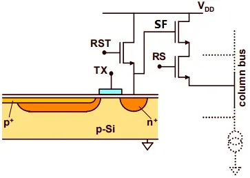
Figure 2: PPD structure
PPD operation sequence:
- Exposure.
- Reset: after exposure, RST is enabled to reset the readout region (n+ region) to a high level.
- Read reset level: read the n+ region level, which includes amplifier offset and 1/f noise and reset-induced kTC noise; store this reading in the first capacitor.
- Charge transfer: enable TX to transfer charge fully from the photodiode region to the n+ region; this mechanism is similar to CCD charge transfer.
- Read signal level: read the n+ region voltage to a second capacitor; this reading includes the photogenerated signal plus amplifier offset, 1/f noise, and kTC noise.
- Signal output: subtract the two capacitor values (CDS) to remove major pixel noise, then perform analog amplification and ADC sampling to produce a digital output.
Advantages of PPD pixels:
- Reset-related kTC noise in the readout region is eliminated by CDS.
- Amplifier offset and 1/f noise are significantly reduced by CDS.
- Reset-induced kTC noise in the photodiode is avoided due to full charge transfer from the PPD.
- Sensitivity depends on depletion width; because the PPD depletion region extends close to the Si-SiO2 interface, PPD sensitivity is higher.
- The p-n-p double-junction structure increases capacitance and supports higher dynamic range.
- A p+ layer covering the Si-SiO2 interface reduces dark current.
Correlated Double Sampling (CDS)
Correlated double sampling (CDS) samples twice: first a reference to evaluate background noise, then after a short delay the target signal. Subtracting the reference from the target removes much of the background noise. The model is shown in Figure 3.
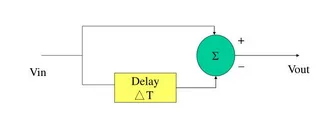
Figure 3: Noise reduction model
CDS works when background noise does not change significantly between the two samples, making it effective against fixed pattern noise (FPN) and low-frequency noise such as 1/f noise and kTC noise.
5. CMOS Sensor Characteristics
A CMOS sensor essentially measures photon conversion events and, in a sense, functions as a photon counter: each pixel value reflects the number of photons captured during a specified time. An ideal sensor would have the following properties:
- Output proportional to input (no sensor noise besides intrinsic signal noise)
- Unlimited input and output ranges
- High sensitivity: small input produces a large output
- High frame rate
- High resolution
- Low power consumption
- Simple process
- Low cost
Figure 4 shows the ideal sensor response. The slope of the linear region in Figure 5 defines the gain: the response produced per unit input. Sensors provide interfaces to adjust the effective gain.
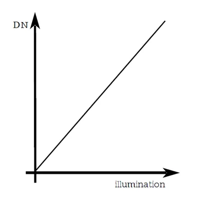
Figure 4: Ideal sensor response
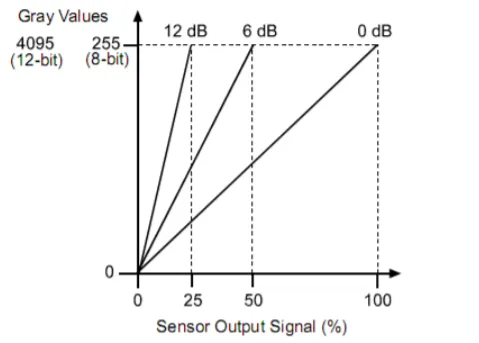
Figure 5: Ideal sensor response curve
Real sensors maintain linear response only within a limited range; for very small or very large inputs the response deviates from linearity, as shown in Figure 6.
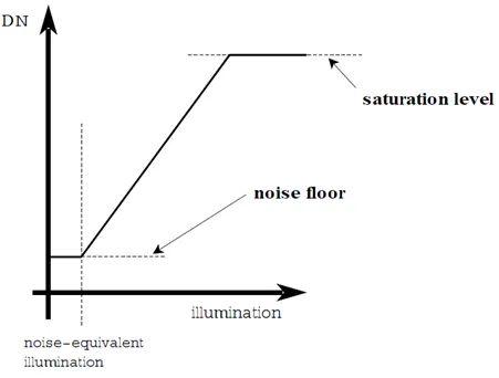
Figure 6: Actual sensor response
6. CMOS Sensor Noise
Assuming constant, uniform illumination, image noise is the sum of spatial and temporal fluctuations in the measured signal. The transfer-function model in Figure 7 summarizes the photonic-to-electrical conversion and the main noise sources mathematically.
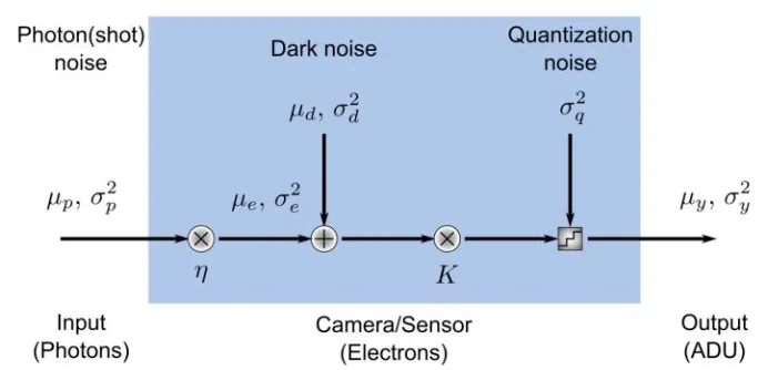
Figure 7: Transfer noise model
Dark Current Noise
Thermal motion in silicon can randomly excite electrons into the conduction band, producing dark current. Even without incident photons, a sensor produces some signal. Random variations in dark current during exposure form dark shot noise. Dark noise follows Poisson statistics, is independent of signal level, and depends strongly on temperature—dark current typically doubles for every 8°C increase. Design should keep heat-generating components away from the sensor to reduce dark current.
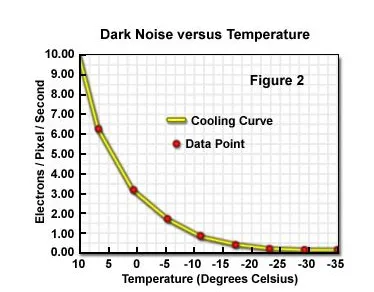
Figure 8: Dark current vs temperature
Readout Noise
Readout noise arises during electronic signal generation. The ADC converts the analog amplifier output to a digital value. Finite ADC resolution (typically 10 to 14 bits) quantizes the analog value, introducing quantization noise, which is a key component of readout noise. Readout noise is determined by sensor design and indicates how many electrons are required to change the ADC output by one bit. It is independent of signal level and sensor temperature.
Shot Noise (Photon Noise)
Shot noise is the statistical noise associated with photon arrival on a pixel. Photon arrival is temporally and spatially random and follows Poisson statistics. Shot noise depends on signal level and is independent of sensor temperature.
Fixed Pattern Noise (FPN)
FPN is caused by spatial nonuniformity across pixels. In CMOS sensors, each pixel has a charge-voltage amplifier, and rows and columns have transistors for reset and readout control. Parameter variations and device mismatches produce fixed patterns of noise. Defective or blemished pixels also contribute to FPN, which can be modeled as in Figure 9.
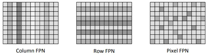
Figure 9: FPN model
Reset Noise
Rolling shutter exposure requires resetting potential wells to clear accumulated charge before the next exposure. Because of dark current, each reset leaves residual random noise—reset noise—typically called kTC noise. Reset amplitude depends on pixel structure, chip temperature, and PN-junction capacitance. Reset requires time; even with relatively large reset currents it can take over 1 ms to fully remove charge.
Practical reset control pulses are often shorter than 1 ms, so remnants of the previous frame can persist into the next frame. This residual image is called image lag, a form of noise.
Crosstalk
In sensor systems, crosstalk refers to incident light intended for pixel A being captured instead by neighboring pixel B, producing unwanted signal in B. Photons can penetrate silicon and reach adjacent pixel photodiodes, creating crosstalk. Figure 10 illustrates a layout where opaque pixels (pink) should have no output but can register signal due to photon penetration, while normal pixels are shown in yellow.

Figure 10: Crosstalk model
7. CMOS Sensor Process Structures
Front-Side Illumination (FSI)
In traditional FSI processes, the photosensitive PN junction sits beneath multiple metal and dielectric layers for filters and microlenses. The circuit stack above the photodiode restricts the photodiode's collection area and acceptance angle, and light may be absorbed or scattered by the circuitry, reducing optical efficiency, as shown in Figure 11.
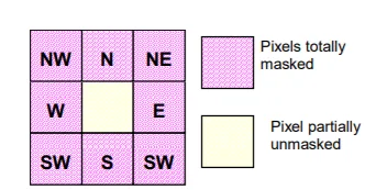
Figure 11: FSI process structure
Back-Side Illumination (BSI)
With semiconductor process advances, wafers can be thinned so light enters from the back side and reaches the photodiode from behind. This back-side illumination (BSI) approach is technically and economically feasible and improves optical efficiency.
8. CMOS Sensor Developments
Sony introduced the first-generation Exmor CMOS image sensor series in 2007. Compared to conventional CIS, Exmor allocated a dedicated ADC and additional CDS per column. Bringing the ADC closer to the pixels and leveraging large-scale parallelism reduces per-unit device frequency and significantly improves noise performance. The added CDS further suppresses noise.
As manufacturing evolved, stacked processes were developed on top of BSI. Stacked sensors place two or more silicon wafers in a vertical stack: the top wafer is used primarily for the pixel photodiodes, while analog and digital control circuitry is moved to lower wafers. This approach allows the photodiode area to occupy nearly 100% of the sensor surface, maximizing optical efficiency.
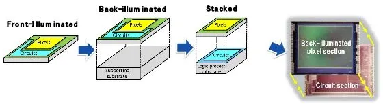
Figure 12: FSI, BSI, Stacked structure comparison
CMOS sensors can also be designed to support global shutter operation. Like CCDs, a global shutter design provides a storage capacitor alongside each exposure pixel so that the entire array exposes simultaneously, then transfers photoelectrons to storage capacitors for locked readout.
DCG is a mode proposed by OmniVision where each pixel can individually control its conversion gain using a CG control. In HDR mode, a single exposure is performed but read out twice: once with high conversion gain (HCG) to capture shadow details and once with low conversion gain (LCG) to capture highlight details.
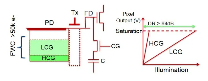
Figure 13: DCG pixel structure