 ALLPCB


Introduction
High-frequency PCBs face significant challenges in maintaining signal integrity as data rates increase and frequencies exceed gigahertz ranges. Through-hole vias, essential for multilayer interconnects, introduce parasitic effects that degrade performance. These effects include signal reflections and impedance discontinuities caused by unused via portions known as stubs. Backdrilling techniques address these issues by precisely removing via stubs during manufacturing. This process, critical for applications like telecommunications and computing, ensures cleaner signal transmission. Electrical engineers must understand backdrilling to optimize designs for reliable high-speed operation.
What Is Backdrilling and Why It Matters for High-Frequency PCBs
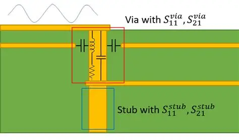
Backdrilling, also called controlled depth drilling, involves drilling out the non-functional stub of a plated through-hole via from the opposite side of the board. In standard through-hole vias, the copper barrel extends fully through the PCB stackup, but only a portion connects active layers. The remaining stub acts as a resonant transmission line at high frequencies, causing reflections and attenuating signals. For high-frequency PCB backdrilling, this removal shortens the via length to match the signal path needs. Signal integrity improves dramatically, reducing bit error rates in high-speed interfaces. Without backdrilling, engineers risk crosstalk and insertion loss, compromising overall system performance.
Via stubs become problematic when their electrical length approaches a quarter wavelength of the signal frequency. At frequencies above 1 GHz, even short stubs generate significant reflections due to impedance mismatch. Backdrilling signal integrity benefits extend to better eye diagrams and lower jitter. Factory processes align this technique with design intent to support dense routing in multilayer boards. Engineers specify backdrilling in stackups to target specific nets carrying critical signals.
Technical Principles of Via Stub Effects and Backdrilling
Signal propagation through a via encounters a sudden impedance change at the stub transition, reflecting a portion of the energy back toward the source. This reflection coefficient depends on the stub length and dielectric properties of the surrounding material. In high-frequency environments, the stub resonates, amplifying noise and distorting waveforms. Backdrilling eliminates this by creating a shorter effective via with minimal residue. Controlled depth drilling ensures the drill stops precisely at the last connected layer, leaving a small annular ring for plating integrity.
The principle relies on precise depth control during secondary drilling after initial via plating. Larger drill diameters, typically oversized relative to the original via, clear the stub while avoiding damage to active connections. This maintains via reliability under thermal stress and mechanical handling. Engineers model these effects using time-domain reflectometry to predict stub impacts pre-manufacturing. PCB manufacturing backdrilling integrates seamlessly into standard workflows, enhancing high-speed viability.
Dielectric materials with low loss tangents complement backdrilling by minimizing additional attenuation. However, the primary gain comes from stub removal, which aligns via impedance closer to trace values. Standards like IPC-6012 outline performance qualifications for such features, ensuring consistency across production.
Related Reading: Backdrilling Design: The Ultimate Guide to Eliminating Via Stubs for High Speed PCBs
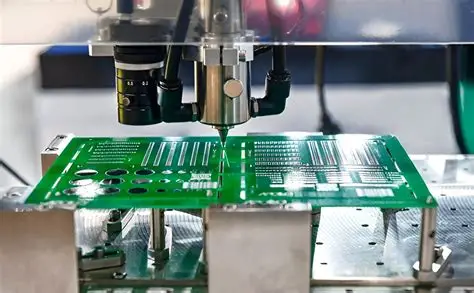
The Backdrilling Process in PCB Manufacturing
The backdrilling process begins after through-hole vias are drilled, plated, and the board is at full stackup thickness. Manufacturers generate separate drill files for backdrill locations, specifying X-Y coordinates and depths per via. A specialized CNC drill machine uses optical registration or fiducials for alignment, employing a larger bit to remove the stub. Depth control mechanisms, such as peck drilling or depth sensors, prevent over-drill into functional layers. Post-backdrill inspection verifies stub removal and checks for residue or breakout.
Plating remains intact on the shortened barrel, preserving electrical continuity. Etch-back processes may follow to clean any exposed copper shoulders. This sequence minimizes defects like nailheading or fiberglass protrusion. High-frequency PCB backdrilling demands tight tolerances to achieve uniform results across panels.
Verification includes cross-section analysis on coupon panels, measuring remaining stub lengths. Electrical testing confirms impedance profiles match simulations. Factories incorporate these steps to meet high-reliability demands.
Key Parameters and Considerations for Controlled Depth Drilling
Successful controlled depth drilling hinges on drill size selection, with backdrill diameters oversized to ensure complete stub clearance without enlarging the via excessively. Depth specification targets the entry side's last land plus a safety margin. Aspect ratios influence feasibility, as deeper boards require stiffer tooling. Manufacturers assess drill wander and breakthrough risks during planning.
Alignment precision is paramount, often using machine vision for sub-thou positioning. Board warpage must stay minimal to avoid depth variations. Pre-drill panel coupons validate process capability per layer depth.
IPC-A-600 provides acceptability criteria for backdrilled features, guiding visual and dimensional checks. Engineers communicate requirements via fabrication drawings, noting backdrill pairs for top and bottom entries.
Benefits of Backdrilling for Signal Integrity
Backdrilling signal integrity enhancements include reduced return loss by eliminating stub-induced reflections. Signals experience less attenuation, enabling longer traces at high data rates. Crosstalk between adjacent vias decreases due to shorter coupling lengths. Impedance control improves, stabilizing time-domain responses.
In high-frequency applications, these gains support protocols demanding clean eye openings. Via stub removal also lowers EMI emissions by confining fields to active paths. Overall, backdrilling extends PCB usability to multi-gigabit speeds without blind or buried vias.
Related Reading: Backdrilling: The Signal Integrity Superhero for High-Speed PCBs
Best Practices for Implementing High-Frequency PCB Backdrilling
Designers should minimize via count by optimizing layer pairing for high-speed nets. Specify backdrills only for critical signals, balancing cost with performance. Provide clear stackup cross-sections in drawings, labeling depths and tolerances.
Manufacturers recommend pilot holes or verification coupons for each unique depth. Simulate backdrill shoulders to ensure plating coverage. Post-process cleaning removes debris, preventing shorts.
Collaborate early with fabricators on DFM reviews. Test prototypes with TDR to validate stub reduction. Adhere to IPC-2221 guidelines for via design in high-speed contexts.
Challenges in PCB Manufacturing Backdrilling and Solutions
Alignment errors can leave residual stubs or damage lands, addressed by advanced registration systems. Depth overshoot risks functional layers, mitigated by real-time monitoring. Larger backdrill bits increase breakout on thin cores, requiring sequential drilling.
Residue from drilling may cause reliability issues, countered by plasma or chemical desmear. Cost rises with multiple depths, so consolidate where possible. Factories train operators on high-frequency PCB backdrilling specifics.
Conclusion
Backdrilling techniques transform high-frequency PCB performance by targeting via stub removal through controlled depth drilling. Electrical engineers benefit from enhanced signal integrity, enabling reliable high-speed operation. Manufacturing processes deliver precision, aligned with industry standards. Integrating best practices ensures optimal results without excessive complexity. Future designs will increasingly rely on this method as frequencies rise.
FAQs
Q1: What is high-frequency PCB backdrilling and when is it necessary?
A1: High-frequency PCB backdrilling removes unused via stubs to prevent signal reflections in multilayer boards operating above 1 GHz. It becomes essential for data rates where stub lengths exceed quarter-wavelength thresholds, such as in DDR4 or PCIe interfaces. Factory processes use controlled depth drilling post-plating for precision. This maintains impedance continuity and reduces jitter effectively.
Q2: How does backdrilling signal integrity improve in high-speed designs?
A2: Backdrilling signal integrity improves by shortening vias, minimizing reflections and insertion loss from stubs. Cleaner waveforms result in better eye diagrams and lower bit error rates. Crosstalk diminishes as coupling paths shorten. Engineers verify via TDR measurements post-manufacturing.
Q3: What are key steps in PCB manufacturing backdrilling?
A3: PCB manufacturing backdrilling starts after PTH plating, using oversized drills from the opposite side to specified depths. Alignment relies on fiducials, with depth control via peck cycles. Inspection includes cross-sections and electrical tests. Coupons validate each depth for consistency.
Q4: Why is controlled depth drilling critical for via stub removal?
A4: Controlled depth drilling ensures precise stub removal without harming active connections, vital for high-frequency performance. It preserves plating on functional barrels while clearing parasitics. Tolerances prevent over-drill, maintaining board integrity. This technique supports dense, reliable interconnects.
References
IPC-6012E — Qualification and Performance Specification for Rigid Printed Boards. IPC, 2017
IPC-A-600K — Acceptability of Printed Boards. IPC, 2020
IPC-2221G — Generic Standard on Printed Board Design. IPC, 2012


