 ALLPCB


Printed circuit boards form the foundation of modern electronic systems, and their reliability depends on thorough inspection processes that go well beyond simple visual checks or basic continuity tests. Engineers working with high-density interconnects and multilayer constructions face increasing challenges from miniaturization and complex component placement. Advanced methods such as 3D AOI PCB inspection provide three-dimensional surface data that reveals subtle defects invisible to two-dimensional systems. These techniques help maintain performance across demanding applications in automotive, aerospace, and telecommunications sectors. Structured evaluation at multiple production stages reduces the risk of field failures and supports consistent manufacturing output.
Why Advanced Inspection Techniques Matter for Electric Engineers
Electric engineers must verify that every PCB meets functional and structural requirements before integration into larger assemblies. Traditional inspection approaches often miss issues like hidden voids or slight height variations that affect signal integrity and thermal performance. Advanced methods deliver quantitative data that supports design validation and process optimization. This level of detail becomes essential when boards incorporate fine-pitch components or operate under elevated temperatures and mechanical stress. Reliable inspection data also assists procurement teams in qualifying suppliers and maintaining traceability throughout the supply chain.
Technical Principles of 3D AOI PCB Inspection
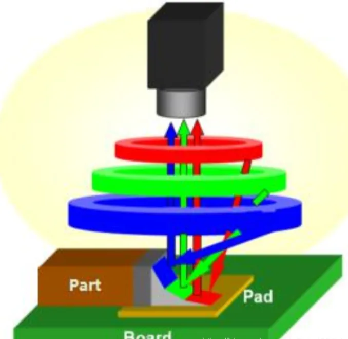
Three-dimensional automated optical inspection systems project structured light patterns onto the board surface and capture reflected images from multiple angles. Algorithms reconstruct height maps that measure solder paste volume, component coplanarity, and lead lift with micrometer-level precision. The process identifies bridging, insufficient solder, and tombstoning that two-dimensional cameras overlook. Engineers interpret the resulting point-cloud data to correlate physical measurements with electrical performance expectations. This approach aligns with established quality criteria that emphasize measurable acceptance limits rather than subjective judgment.
Related Reading: Beyond Visuals: How 3D AOI is Revolutionizing PCB Defect Detection
Mechanisms Behind Thermal PCB Inspection
Thermal inspection relies on infrared imaging or contact sensors to map temperature distribution across operating boards. Engineers apply controlled power cycles and observe heat flow patterns that indicate poor thermal vias, delamination, or uneven copper distribution. The technique detects localized hot spots that could accelerate material degradation over time. Data collection occurs under simulated load conditions to mirror real-world operating environments. Analysis of thermal gradients helps refine layout decisions and material selections during the design phase.
How Flying Probe Testing Works
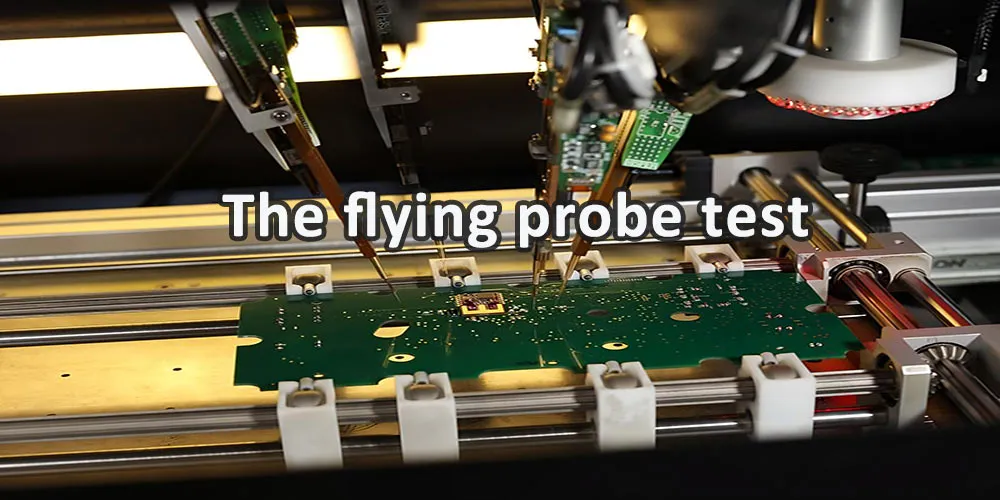
Flying probe testing uses movable probes that contact test points without requiring a dedicated fixture. The system moves probes in programmed sequences to perform in-circuit measurements of resistance, capacitance, and diode characteristics on bare or assembled boards. Engineers configure test programs to cover high-density areas where bed-of-nails fixtures become impractical. The method supports rapid iteration during prototype validation and low-volume production runs. Measurement accuracy depends on precise probe positioning and controlled contact force to avoid surface damage.
Related Reading: The Ultimate Guide to PCB Inspection: Techniques and Technologies
Microsection Analysis for Internal Structure Verification
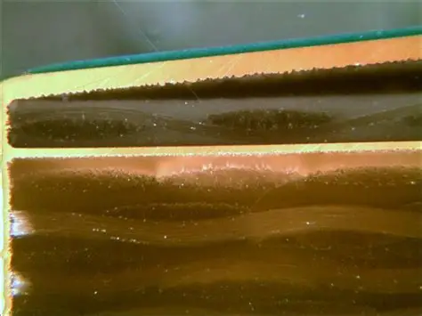
Microsection analysis involves cutting a representative sample from the board, mounting it in resin, and polishing the cross-section to expose internal layers. Engineers examine the polished surface under a microscope to measure plating thickness, via fill quality, and laminate integrity. The procedure reveals defects such as resin voids, glass fiber exposure, and copper dissolution that surface inspections cannot detect. Controlled etching steps enhance contrast between different material layers for accurate dimensional assessment. Results provide objective evidence that supports acceptance decisions according to documented criteria.
Best Practices for Implementing Advanced Inspection
Engineers integrate these techniques into a staged inspection plan that begins with incoming material verification and continues through final assembly. Selection of the appropriate method depends on board complexity, production volume, and the criticality of the end application. Consistent calibration of equipment and standardized operating procedures ensure repeatable results across different shifts and facilities. Documentation of inspection parameters and findings supports root-cause analysis when anomalies appear. Regular review of accumulated data helps identify process trends and drive continuous improvement initiatives.
Practical Insights for Electric Engineers
Combining 3D AOI PCB inspection with thermal PCB inspection and flying probe testing creates a comprehensive quality gate that addresses both surface and electrical characteristics. Microsection analysis serves as a confirmatory tool when initial results indicate potential internal issues. Engineers document each step to maintain traceability and facilitate communication between design, manufacturing, and quality teams. This layered approach reduces escaped defects and strengthens overall product reliability without introducing unnecessary production delays.
Conclusion
Advanced PCB inspection methods extend quality assurance capabilities well beyond conventional limits. Techniques including 3D AOI PCB inspection, thermal PCB inspection, flying probe testing, and microsection analysis supply the detailed measurements required for modern high-reliability boards. Electric engineers who apply these methods systematically achieve higher first-pass yields and lower warranty returns. Continued refinement of inspection protocols remains essential as board densities and performance expectations continue to rise.
FAQs
Q1: What distinguishes 3D AOI PCB inspection from traditional two-dimensional methods?
A1: Three-dimensional automated optical inspection captures height information in addition to planar images, enabling precise measurement of solder volume and component coplanarity. Engineers use the resulting data to identify defects such as insufficient paste or lead lift that affect long-term reliability. The technique integrates into production lines to provide quantitative feedback for process adjustments. Consistent application supports compliance with acceptance criteria defined in industry standards.
Q2: How does thermal PCB inspection help identify potential reliability issues?
A2: Thermal PCB inspection maps heat distribution under operating conditions to reveal hot spots caused by poor thermal paths or material inconsistencies. Engineers compare observed patterns against expected thermal profiles derived from design simulations. Early detection of anomalies allows corrective actions before boards enter field service. The method complements electrical testing by highlighting degradation mechanisms that appear only under load.
Q3: When should engineers consider flying probe testing instead of fixture-based methods?
A3: Flying probe testing offers flexibility for prototype boards and low-volume runs where creating a dedicated test fixture would be cost-prohibitive. Engineers program probe movements to access dense test points without mechanical interference. The approach maintains measurement accuracy while accommodating design changes during development. It also supports rapid verification of both bare boards and assembled units.
Q4: What information does microsection analysis provide that other inspection techniques cannot?
A4: Microsection analysis exposes internal features such as plating thickness and via fill quality through controlled cross-section preparation. Engineers measure these dimensions directly to confirm conformance with structural requirements. The method detects subsurface defects including delamination and resin starvation that remain invisible to surface-based inspections. Results contribute to overall process validation and material qualification activities.





