 ALLPCB


Introduction
The demand for compact, high-performance electronics has made 6-layer PCBs a staple in applications ranging from telecommunications to automotive systems. These multilayer boards offer enhanced signal integrity and power distribution compared to simpler designs, but their assembly introduces unique challenges due to increased thickness and complexity. Mastering the 6-layer PCB assembly process ensures reliable manufacturing outcomes, minimizing defects like voids or misalignment. This article breaks down best practices for electric engineers, focusing on soldering techniques, component placement, inspection, and rework. By following these guidelines, teams can achieve consistent quality in production runs. Practical insights drawn from industry-standard procedures will help troubleshoot common issues effectively.
Understanding 6-Layer PCBs and Assembly Challenges
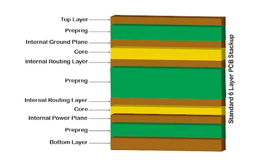
A 6-layer PCB consists of six copper layers separated by dielectric materials, typically arranged as signal-ground-signal-power-ground-signal to optimize impedance control and reduce crosstalk. This stackup supports dense routing and dedicated planes for power and ground, essential for high-speed signals. During assembly, the board's thickness, often around standard rigid board profiles, heightens risks like warpage from thermal stresses or via misalignment. Engineers must account for these factors early to prevent yield losses. The assembly process demands precision in handling multilayer interactions, where inner layer integrity affects outer component performance. Addressing these upfront through design-for-assembly principles sets the foundation for success.
The 6-Layer PCB Assembly Process Step-by-Step
The 6-layer PCB assembly process begins with solder paste printing, where stencil alignment ensures uniform deposition on pads, critical for fine-pitch components. Next, automated pick-and-place machines position surface-mount devices (SMDs) accurately, using fiducials on the board for registration. Reflow soldering then melts the paste to form joints, followed by through-hole insertion if mixed technology is used. Post-reflow cleaning removes flux residues to avoid ionic contamination. Final steps include conformal coating application and functional testing. Each stage requires controlled environments to maintain multilayer planarity and prevent delamination.
6-Layer PCB Soldering Techniques
Effective 6-layer PCB soldering techniques prioritize reflow profiles tailored to the board's thermal mass, ensuring even heating across layers without overheating inner planes. Nitrogen atmospheres reduce oxidation, promoting reliable wetting on pads and vias. For mixed SMT and through-hole, selective soldering targets pins while sparing nearby SMDs. Avoiding solder balls or bridging involves precise stencil apertures and paste volume control. These methods align with requirements in J-STD-001, emphasizing material compatibility and process verification. Troubleshooting overheating starts with thermal profiling to adjust conveyor speed and zone temperatures dynamically.
Component leads must form smooth fillet shapes post-soldering, indicating proper flow. Engineers often profile multiple boards to map heat distribution variances due to copper planes. Post-solder inspection flags incomplete reflow early.
6-Layer PCB Component Placement Guidelines
6-layer PCB component placement guidelines emphasize grouping high-speed signals near dedicated planes to minimize loop inductance. Place BGAs and fine-pitch ICs on outer layers for easier access, avoiding inner layer shadowing from vias. Maintain adequate spacing between power devices and sensitive analog components to reduce noise coupling. Fiducial marks and panelization aid machine vision alignment, compensating for board warp. Decoupling capacitors should sit as close as possible to power pins, ideally under 1mm away where feasible. These practices enhance signal integrity while simplifying rework access.
Symmetrical placement across the board mitigates warpage during reflow. Engineers simulate thermal loads pre-production to refine layouts.
6-Layer PCB Inspection Methods
6-layer PCB inspection methods combine automated optical inspection (AOI) for surface defects with X-ray for hidden solder joints under BGAs. AOI verifies paste volume, bridges, and tombstoning post-placement, while X-ray reveals voids in vias or balls. Functional testing follows, probing nets for continuity and shorts. Adhering to IPC-A-610 criteria classifies acceptability by class, from general consumer to high-reliability aerospace. Manual visual checks supplement automation for subtle issues like fillet concavity. Layered inspections catch multilayer-specific faults, such as inner plane shorts from drilling debris.
In-line flying probe tests verify high-density nets efficiently. Data logging trends defects for process tweaks.
6-Layer PCB Rework Procedures
6-layer PCB rework procedures demand localized heating to avoid stressing adjacent layers, using hot air or infrared tools for SMD removal. For BGAs, precise alignment during reballing prevents offset, with reflow ovens for final attachment. Pad cleaning follows component lift-off, repairing damaged lands if needed. IPC-7711/7721 outlines steps for modification and repair, stressing temperature control and flux selection. Post-rework, re-inspection confirms joint integrity without board damage. Documenting each intervention tracks reliability impacts for future prevention.
Thermal profiling during rework simulates production conditions. Multi-layer access requires bottom-side support to prevent flexing.
Common Challenges and Troubleshooting in 6-Layer Assembly
Warpage tops challenges in 6-layer assembly, arising from asymmetric copper distribution or CTE mismatches during reflow. Measure bow and twist pre-assembly, baking boards to remove moisture. Solder voids under BGAs signal trapped flux; extend preheat times or switch low-residue pastes. Misalignment from placement jitter worsens with board thickness; calibrate machines and use rigid carriers. Bridging in dense areas calls for finer stencils and shear-thinning pastes. Systematic root-cause analysis, like failure mode effects, resolves recurring issues practically.
Conclusion
Reliable 6-layer PCB manufacturing hinges on integrating precise processes with proactive troubleshooting. From optimized soldering and placement to rigorous inspections and controlled rework, each step builds toward defect-free assemblies. Electric engineers benefit from standard-aligned practices that enhance yield and longevity. Implementing these best practices reduces downtime and supports scalable production. Focus on process control and data-driven adjustments for consistent results. Ultimately, demystifying assembly empowers teams to tackle complexity confidently.
FAQs
Q1: What are the key steps in the 6-layer PCB assembly process?
A1: The 6-layer PCB assembly process starts with solder paste printing via stencils, followed by high-precision component placement using fiducials. Reflow soldering forms joints, with cleaning and through-hole wave soldering if required. Inspection via AOI and X-ray ensures quality before testing. This sequence minimizes multilayer defects like voids or warpage, promoting high yields in production.
Q2: How do 6-layer PCB soldering techniques differ from simpler boards?
A2: 6-layer PCB soldering techniques account for greater thermal mass, using profiled reflow with nitrogen to ensure even heating across planes. Selective soldering handles mixed tech without disturbing SMDs. Flux choice and stencil design prevent bridging in dense areas. These align with J-STD-001 for robust joints, addressing warpage risks unique to multilayers.
Q3: What 6-layer PCB component placement guidelines improve reliability?
A3: Prioritize outer layers for high-speed ICs and BGAs, with decoupling caps near power pins. Use fiducials for alignment and space components to cut noise. Symmetrical layouts reduce thermal warp. These guidelines enhance signal integrity and ease inspection in 6-layer designs.
Q4: Which 6-layer PCB inspection methods detect hidden defects?
A4: AOI catches surface issues like bridges, while X-ray reveals BGA voids and via fills in 6-layer PCBs. IPC-A-610 criteria guide acceptability checks. Functional probing verifies nets. Combining methods ensures comprehensive multilayer validation.
Q5: What are standard 6-layer PCB rework procedures for BGAs?
A5: IPC-7711/7721 guides BGA rework: remove with hot air, clean pads, reball, and reflow with alignment. Control heat to spare layers. Re-inspect joints post-procedure. This prevents damage in dense 6-layer assemblies.


