ALLPCB


Introduction
As Moore's Law approaches physical limits, integrating more devices onto a single chip has become increasingly challenging. New architectural approaches to integrated circuit design are needed. This article explains a 3D-view design concept for integrated circuits from an architecture and EDA perspective.
1. Designing Integrated Circuits from a 3D View
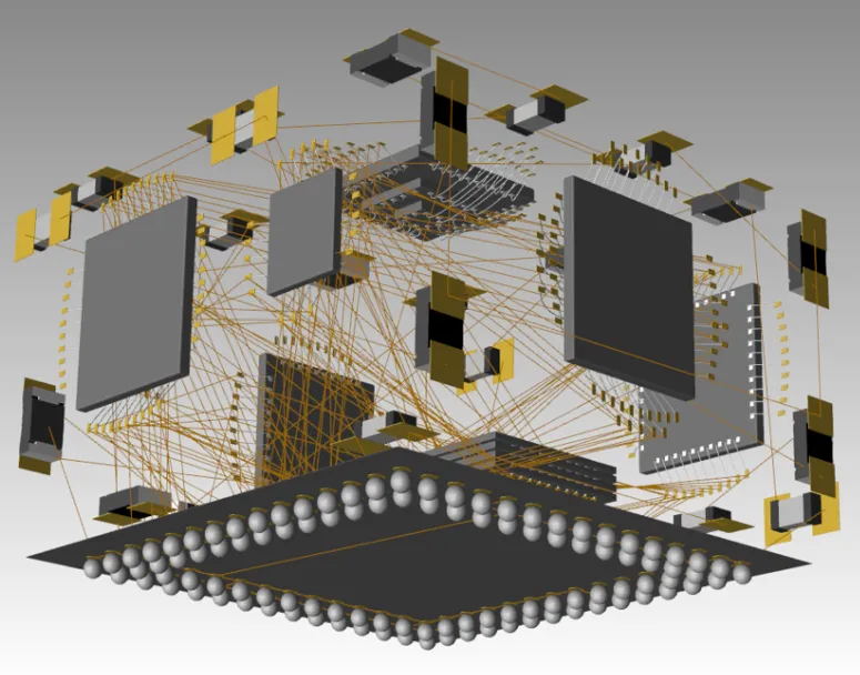
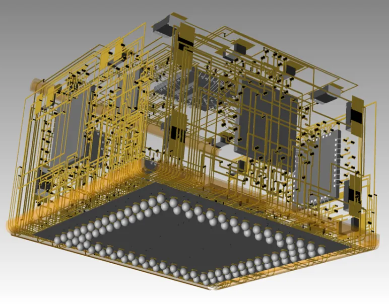
In traditional large-scale integrated circuit design, the entire electronic system is integrated on a single chip: microprocessor, analog IP, digital IP, memory and off-chip memory interfaces are placed on the same wafer plane and usually manufactured in the same process. Transistors are all located on a single plane, carved into the wafer surface at nanoscale. As systems become more complex, die area increases and yield typically falls. With process nodes approaching physical limits, Moore's Law becomes harder to sustain. Package-level solutions such as SiP, advanced packaging, chiplets and heterogeneous integration have emerged as ways to extend functionality.
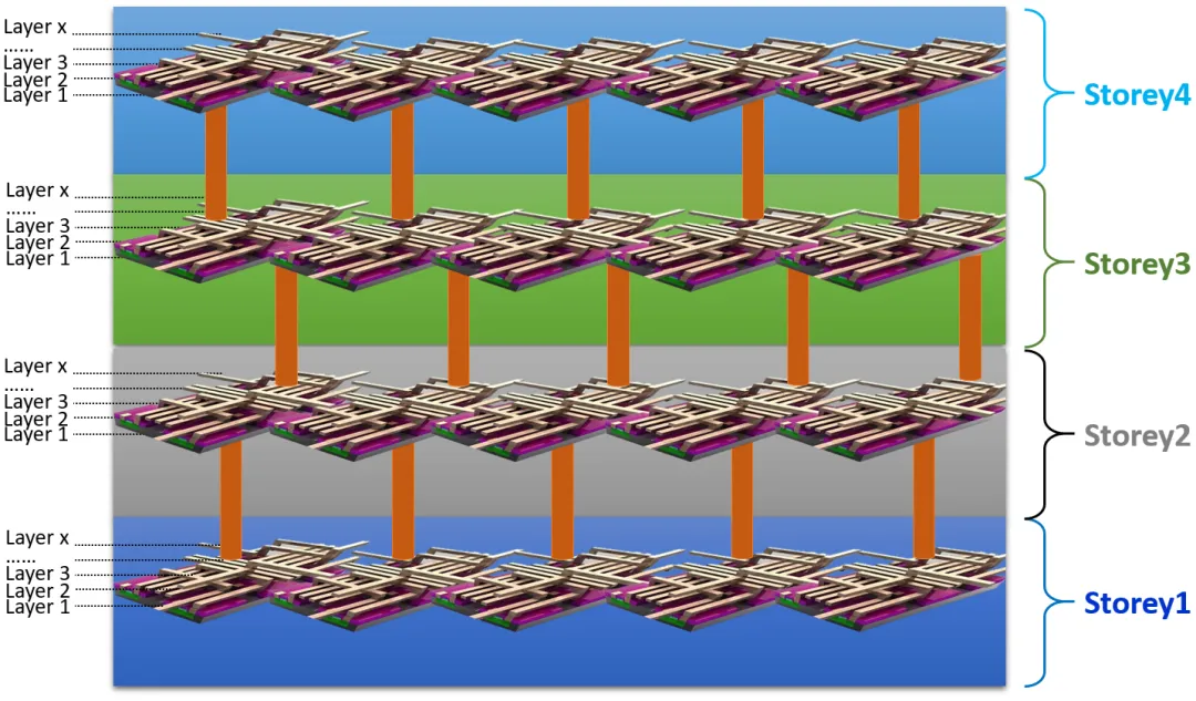
This article proposes a further step: design integrated circuits from a 3D viewpoint. Instead of placing the CPU, analog IP, digital IP and memory on the same wafer plane, design them on different storeys and stack these storeys to form a complete chip. Each storey contains a transistor layer and multiple metal routing layers. Inter-storey interconnects use TSV and patterned redistribution layers (RDL) when needed for alignment. Different storeys may be manufactured in different process nodes; transistors within a single storey must use the same node.
Traditionally, inter-storey interconnects are considered part of advanced packaging. The proposed approach requires considering 3D integration from the initial IC design stage. Because integrated circuit design relies on EDA tools, the main difficulty of this new approach lies in EDA. This effectively requires a convergence of IC design and advanced packaging design, starting with the convergence of EDA tools.
2. New Requirements for EDA Tools
Conventional IC layout tools design transistors, resistors and capacitors on the silicon substrate and then connect them with multiple metal layers, all within a single storey. With multiple storeys, EDA tools must consider both intra-storey and inter-storey signal interconnect and routing. Networks and routing become three-dimensional; we can call them 3D networks and 3D routing. Current EDA tools do not natively support multi-storey layout, so a new class of tools is needed to optimize networks across stacked layout instances situated at different storeys in space.
An IC layout tool must be capable of multi-layout network optimization, managing multiple layout instances either within a single design environment or across coordinated environments, with unified data exchange and control. While no full IC layout tool with this capability exists today, similar capabilities have appeared in advanced packaging design tools that support collaborative multi-die layouts.
Simulation and verification tools must also evolve. They must correctly parse complex 3D design data models, support stronger algorithms for accurate simulation results, and ensure correctness and fidelity from design to production data.
3. Cubic IC Design Methodology
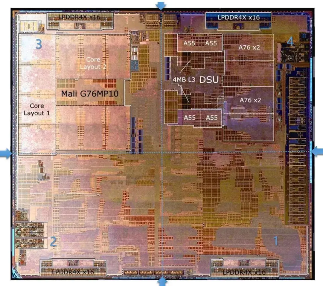
The proposed 3D structure differs from conventional wafer-plane ICs. We name it "Cubic IC", abbreviated CIC. Because a CIC contains multiple device layers, its design methodology differs from traditional IC design. In conventional layout, functional modules are arranged in 2D across the die. For example, the Kirin 980 layout can be partitioned and each partition placed on a different storey and virtually stacked.
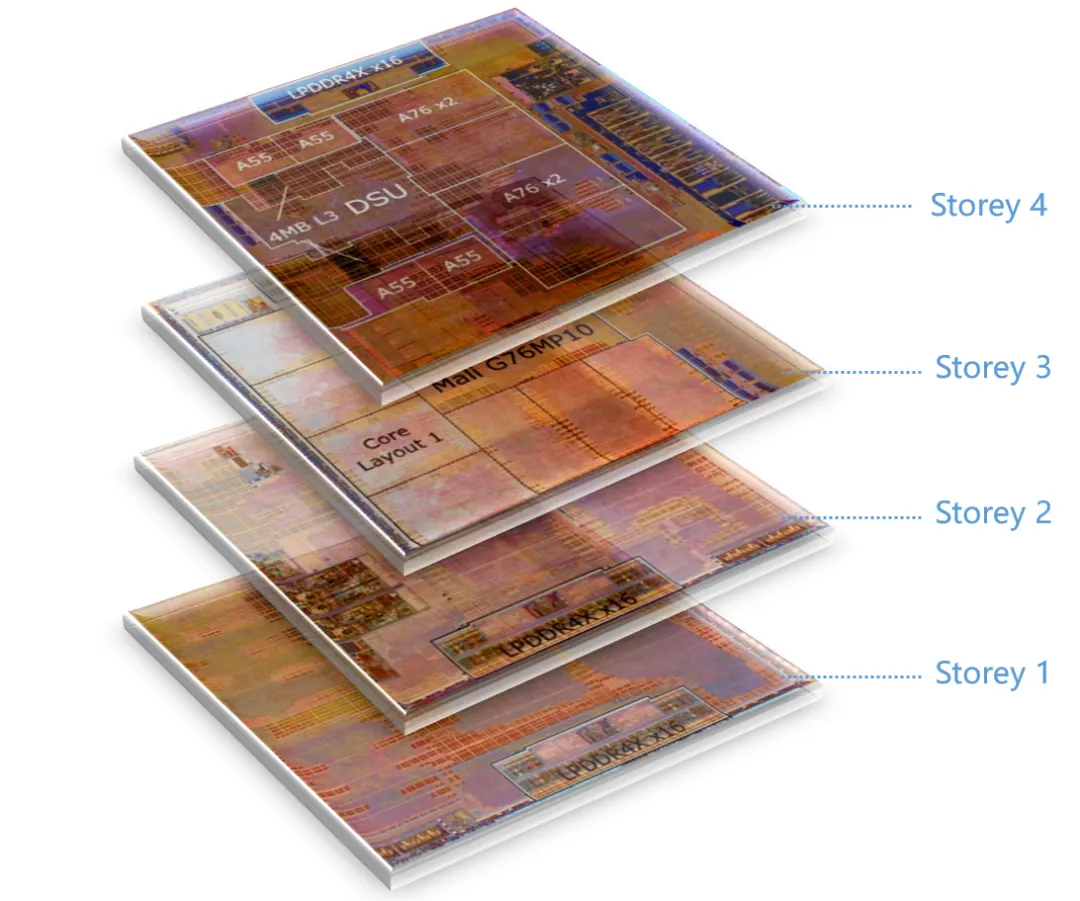
Each storey is designed similarly to a traditional IC layout. Storeys are connected by TSV and RDL, and the overall layout requires global planning. By partitioning and stacking, the chip footprint can shrink; intra-module interconnect distances can decrease, improving performance.
How many layers can be stacked? As storeys increase, XY footprint shrinks until the total stack thickness approaches the die length/width, forming a cube — hence the name Cubic IC. For a fingertip-sized CIC (10 mm by 10 mm), if each storey is thinned to 50 μm, up to about 200 layers can be stacked to form a cube. Exceeding a cubic shape toward a tall column is not recommended, as explained below. In CIC design, total thickness should ideally not exceed the die length or width; a flattened cube is preferred to a tall column.
If die length and width are unequal, maximum thickness should be the smaller of the two. Keeping length and width equal maximizes material utilization. The cubic limit relates to signal propagation distance. In planar transmission, the ideal region reachable in one clock cycle is a circle; as clock rate increases, the reachable radius shrinks and may become smaller than the die area, creating on-chip memory-wall-like limitations. Extending into the Z axis reduces average interconnect distance and can minimize energy for signal propagation until a cube is reached. Beyond that, a taller column increases energy and reduces performance, contradicting design goals.
4. Li's Isochronous Transmission Space (LITS)
To describe signal propagation within a CIC's 3D space, the concept of Li's Isochronous Transmission Space, or LITS, is introduced. LITS is a conceptual space between ideal and realistic transmission ranges, useful when planning 3D IP placement for timing-sensitive designs.
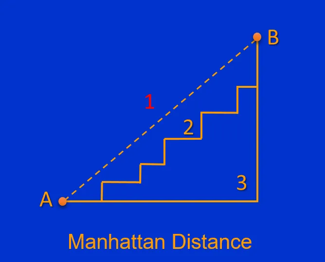
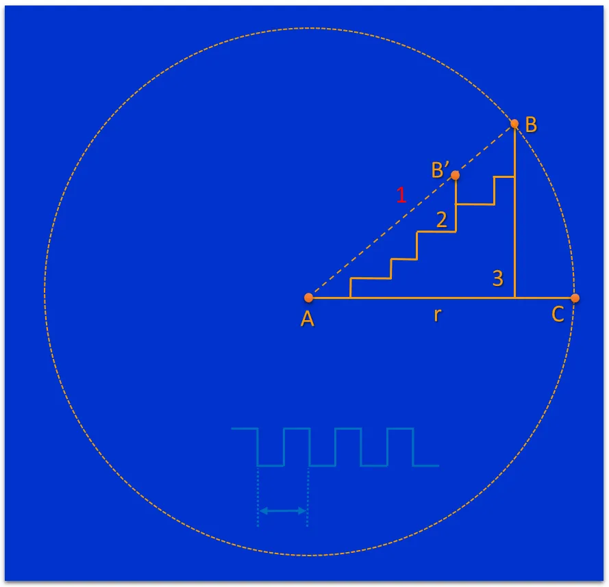
4.1 Manhattan Distance
Manhattan distance measures the sum of absolute axis-aligned distances between two points in Cartesian coordinates. On the XY plane, the Manhattan distance between points A and B equals the sum of their X and Y projections.
4.2 Isochronous Transmission Area (2D)
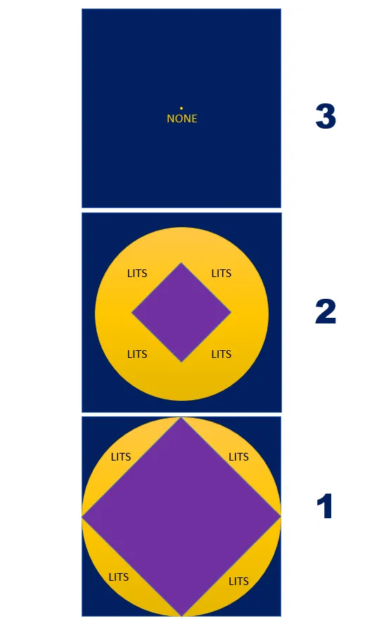
On a planar chip, ideal propagation in one clock cycle is a circle of radius r. However, actual routing typically follows axis-aligned metal directions, so actual reachable points are bounded by Manhattan distance. For origin A, the set of points satisfying |x| + |y| = r forms a 45-degree-rotated square (diamond). If some diagonal routing is allowed, the reachable area lies between this diamond and its circumscribed circle. This practical reachable area is the isochronous transmission area, ITA.
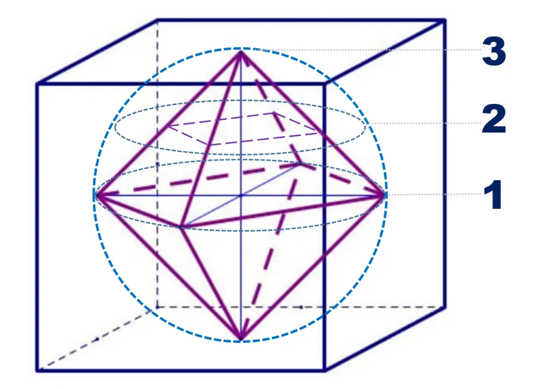
4.3 LITS in 3D
In 3D, routing follows axis-aligned directions along X, Y and Z. The space Manhattan distance is |x| + |y| + |z| = r, which describes a regular octahedron surface. The ideal transmission surface is a sphere. The region between the inscribed octahedron and the sphere is LITS. Quantitatively,
LITS = (4/3) (π - 1) r^3,
and the fraction of the cube volume represented by LITS is
(4/3) (π - 1) r^3 ÷ (8 r^3) ≈ 0.36.
Thus, approximately 36% of the virtual CIC cube lies between practical isochronous transmission and ideal spherical transmission. LITS can guide 3D IP placement: modules with tight equal-length timing requirements should be placed near the inner surfaces of the octahedron for easier physical equal-length routing. LITS projections on different Z planes help partition IP locations. LITS can be constructed around any reference point to analyze signal delay precisely.
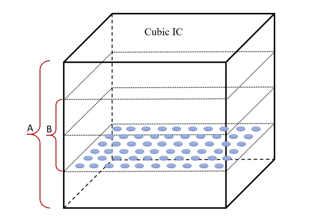
5. Effective Function Volume (EFV)
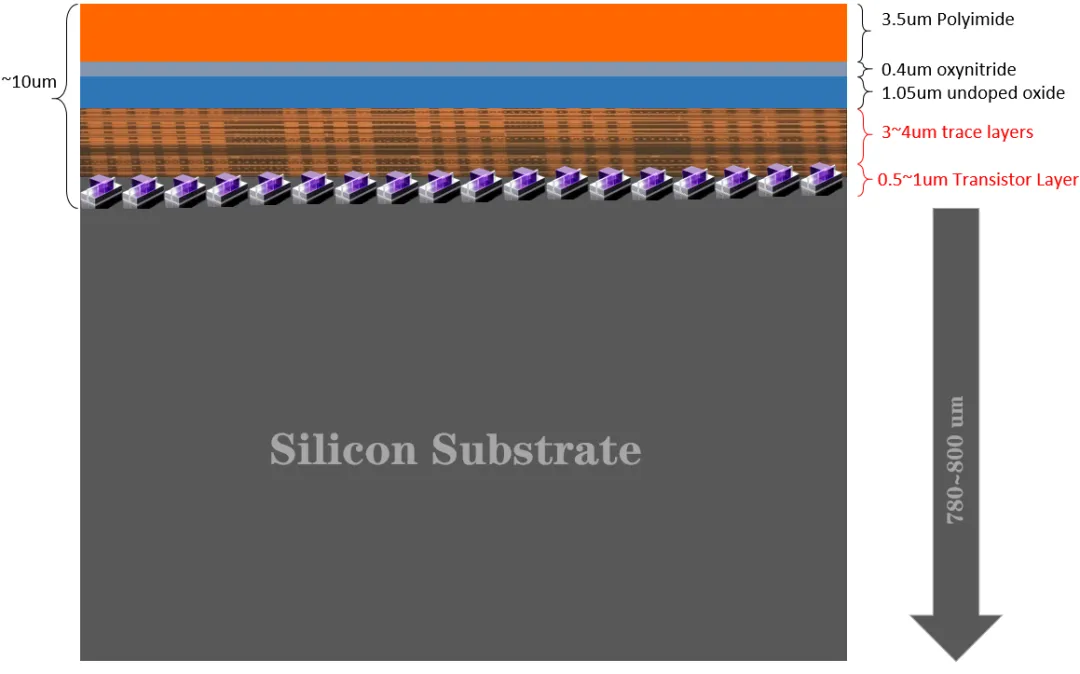
An integrated circuit's function is implemented by transistors grouped into function cells, function blocks and function units. The volume occupied by these function units is the effective function volume, EFV. Much of a chip's physical volume serves as support or protection and is not functional. For example, a typical transistor plus routing region has a total thickness of about 5 μm; above it are insulation and protection layers (polyimide, oxynitride, undoped oxide) totaling about 5 μm. Beneath the transistor layer is the silicon substrate, roughly 780–800 μm thick. In that case, EFV represents about 0.625% of the chip volume.
Thinning the wafer increases EFV fraction. If the wafer is thinned to 100 μm, EFV becomes about 5% of the volume; to 50 μm, EFV ≈ 10%; to 20 μm, EFV ≈ 25%. Twenty micrometers is near current thinning limits. Wafer thinning can increase effective functional density by up to 40× compared with an unthinned substrate, which explains why advanced packaging and heterogeneous integration are sometimes seen as extending Moore's Law. However, this is not a true continuation of Moore's Law, which is inherently limited. When designing systems from function cells up to large systems, analyze EFV at each level and maximize EFV fraction where possible.
6. Differences between Cubic IC and 3D Chiplet
CIC and 3D chiplet approaches both stack partitioned dies and use TSV and RDL for electrical interconnect, but they differ:
- CIC is designed from a 3D viewpoint from the start; 3D chiplet integration typically considers interfaces and then stacks dies at packaging time.
- Storeys in a CIC are identical in size to form a cube; 3D chiplets can have different die sizes.
- CIC is a design and manufacturing vision for future ICs; 3D chiplets are a current advanced packaging and heterogeneous integration implementation.
- Chiplets are an IP-to-die approach: IPs are turned into small dies and integrated at the package level. CIC allocates IPs across storeys rather than splitting them into separate dies.
- CIC could stack hundreds of storeys; current 3D chiplet stacks are typically single-digit layers.
- CIC places much higher demands on EDA tools and currently lacks full tool support; 3D chiplets are supported by existing advanced packaging design tools.
- CIC aims for much higher functional density, and its implementation challenges are accordingly greater.
In summary, CIC can be viewed as a long-term ultimate goal for 3D IC evolution, while 3D chiplets are an intermediate, implementable stage.
7. Expected Manufacturing Flow for Cubic IC
IC manufacturing processes can be categorized broadly into additive processes, subtractive processes, and auxiliary processes. Additive processes add material (e.g., sputtering); subtractive processes remove material (e.g., etching); auxiliary processes such as lithography pattern structures.
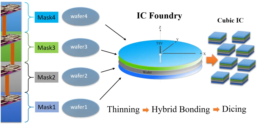
A practical CIC manufacturing flow can mirror conventional wafer processing for each storey: generate masks for each storey; perform lithography, etch, deposition, implantation, CMP, cleaning, etc.; create TSVs for inter-storey interconnects on each wafer; thin wafers to target thickness; and bond wafers together using hybrid bonding. Finally, dice the stacked assembly into individual CIC devices.
8. Challenges Introduced by Cubic IC
All innovations bring new challenges. CIC raises significant challenges in design, manufacturing and thermal management.
8.1 Design Challenges
Main challenges are EDA tool capability and designer productivity. CIC massively increases design complexity. Current chips may have a dozen metal layers above transistors; a CIC could contain hundreds of transistor layers and thousands of metal layers in aggregate. EDA tools must handle such multi-storey designs and manage multiple process node data within one project when different storeys use different nodes. This is a substantial tool development challenge.
For designers, transistor counts scale dramatically. For example, at 7 nm, a fingertip-sized 1 cm^3 CIC may integrate roughly 2.5–5 trillion transistors; with further scaling the transistor count could exceed 1 quadrillion, orders of magnitude higher than current chips. Handling such massive data is a major design and tooling challenge.
Electromagnetic interference is a concern. However, inter-storey transistor spacing after thinning and hybrid bonding is on the order of 20–40 μm, while intra-storey routing spacing is on the order of 20–40 nm, a difference of roughly three orders of magnitude. EMI problems are therefore likely to appear first within a storey and can be addressed using established IC mitigation techniques.
8.2 Manufacturing Challenges
Manufacturing CIC requires reliable TSV formation on each storey and accurate alignment between storeys. If direct TSV alignment is not possible, RDL can be used to assist alignment. Hybrid bonding currently supports interconnect pitch down to about 10 μm, providing about 10,000 interconnects per mm2; future improvements could enable up to 1,000,000 interconnects per mm2, meeting CIC interconnect density requirements.
8.3 Thermal Challenges
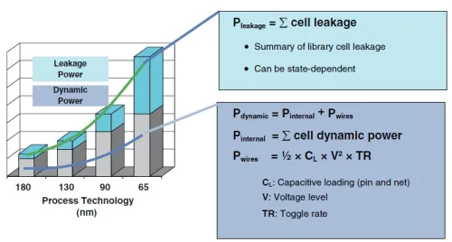
High functional density and vastly increased transistor counts raise heat dissipation challenges. These can be addressed through two main approaches: reducing chip power (dynamic, static and interconnect power) and reducing thermal resistance of heat paths (new thermal materials and structures). Historical concerns about unmanageable chip temperatures have been resolved previously through engineering. CIC thermal design requires careful power reduction and improved thermal channels to dissipate heat effectively.
Conclusion
This article introduced several key concepts: Cubic IC (CIC), isochronous transmission area (ITA), Li's Isochronous Transmission Space (LITS) and effective function volume (EFV). CIC design and manufacturing present substantial technical challenges and will require significant research and development effort.