ALLPCB


Introduction
Low-power chip design has become one of the most important design methodologies of this century. Without low-power techniques, modern smartphones, mobile devices, IoT and many high-performance computing products would not be feasible. As feature sizes shrink, low-power design will play an increasingly important role throughout system-on-chip (SoC) development. Low-power techniques permeate the entire SoC flow, so understanding them in depth is essential for advancing in chip design.
1. Purpose of Low-Power Design
1.1 Origins of Low-Power Techniques
Looking back at three stages of chip-design evolution, each technique emerged to solve specific problems:
- Stage 1—addressing design complexity: in the 1980s, logic synthesis tools greatly improved design productivity;
- Stage 2—scaling size and frequency: in the 1990s, IP reuse enabled large SoCs to reach market quickly while clock frequencies rose from tens of MHz to GHz. Design practices centered on timing and clocks, e.g., timing-driven synthesis and placement-and-routing;
- Stage 3—low-power design: in the 21st century, it became clear that simply increasing clock frequency no longer improved overall system performance. Rising power led to problems such as higher chip temperatures, degraded circuit performance, and power and signal-noise management. The rise of mobile devices, especially phones, accelerated the adoption of low-power chip design.
If low-power techniques were not applied, power would trend upward significantly over technology generations. Intel in 1999 visualized processor power density increasing with time, showing an unsustainable trend where power density could approach extreme levels. That concern led to the belief at the time that 35 nm was a practical limit.
In practice, process development continued to 7 nm and beyond, thanks in large part to low-power design techniques that helped extend the benefits of Moore's Law and enabled today's semiconductor growth.
1.2 Objectives of Low-Power Design
Power and energy are distinct concepts that are often confused. Power is an instantaneous quantity; energy is consumption over time.
Energy = Power * Time
For example, a larger battery (more energy) yields longer device runtime; lower power draw also extends runtime. Therefore, the primary goals of low-power design are:
- Extend runtime of battery-powered electronic products;
- Improve device reliability;
- Reduce cost.
Higher power generates heat more quickly, increasing demands on packaging and thermal solutions. Low-power designs may operate with simple plastic packages and passive cooling, while high-power designs might require ceramic packages, water cooling, or heat spreaders, all of which raise cost. Cost competitiveness directly affects commercial success: a high-function product that is too expensive compared with alternatives will struggle in the market.
Low-power considerations affect many aspects of chip design and are now integral across front-end and back-end flows. Understanding low-power techniques is therefore crucial.
2. Power Components
Low-power techniques are a collection of methods to reduce power. Before discussing techniques, the composition of power must be understood.
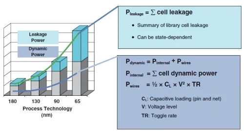
A SoC's power consumption comprises two main parts: dynamic power and static power.
Dynamic power is consumed when a device is active or signals change.
Static power is consumed while the device is powered but signals do not change.
Note: while the device is running, static power is still present because the device is powered. Separating static power is useful for analysis.
2.1 Dynamic Power
Dynamic power includes:
- Switching power (sometimes called toggle power);
- Short-circuit power (also referred to as internal power).
2.1.1 Switching Power
Switching power is the energy required for a gate to charge and discharge its output capacitance when the output transitions between logic levels. In practice, switching power is the dominant component of dynamic power.
Consider a CMOS inverter driving an output capacitance. Each 0-to-1 transition charges the capacitor to Vdd, consuming energy 1/2 * C * Vdd^2, and the 1-to-0 transition discharges that energy to ground. The average switching power can be expressed as:
P = C_L * Vdd^2 * f
where C_L is the load capacitance, Vdd the supply voltage, and f the switching frequency. Often f is represented as f_clock * P_trans, where P_trans is the probability of a transition per clock cycle.
Defining effective capacitance C_eff = C_L * P_trans gives the commonly used form:
P = C_eff * Vdd^2 * f_clock
Key implications from this formula:
- Switching power depends on voltage, toggle rate, and load capacitance;
- Switching power is independent of the actual data values, but depends on transition probability;
- Switching power is independent of the bit-width of a particular transfer operation.
To reduce switching power, the options are:
- Reduce supply voltage Vdd;
- Reduce transition rate (toggle probability);
- Reduce load capacitance.
These measures must be balanced against functional requirements. For example, voltage cannot be reduced to zero, signals must still transition as required, and capacitances cannot be eliminated entirely.
2.1.2 Internal (Short-Circuit) Power
Short-circuit power arises because input transitions are not instantaneous. During a switching event, both PMOS and NMOS devices can conduct simultaneously for a brief interval, creating a direct current path from Vdd to ground. This short-circuit current contributes to dynamic power.
Short-circuit power adds a term to total dynamic power, but since the overlap duration is usually very short, short-circuit power is often much smaller than switching power and may be neglected in first-order estimates. However, in some cases—such as when handling outputs of gated modules—short-circuit power should be considered.
2.2 Static Power
Static power is mainly due to leakage currents. In CMOS gates, leakage comes from several sources:
- Subthreshold leakage (ISUB): current that flows when a transistor is supposed to be off;
- Gate leakage (Igate): tunneling currents through thin gate dielectrics;
- Gate-induced drain leakage (IGIDL): junction-related leakage when source/drain regions are at different potentials relative to the substrate;
- Reverse-bias junction leakage (IREV): generated by minority-carrier diffusion and generation in depletion regions.
MOS transistor structure and leakage contributions vary by process node.
2.2.1 Subthreshold Leakage
Subthreshold leakage occurs when a transistor is not fully off. A representative relationship shows exponential dependence on Vgs and threshold voltage Vth. W/L and process-related parameters (Cox, Vth) determine magnitude. Increasing threshold voltage reduces subthreshold leakage but degrades switching speed and increases delay.
Practical points:
- Reducing Vdd or increasing Vth reduces leakage;
- Increasing Vth causes performance loss and must be applied only when functional requirements permit;
- Subthreshold leakage depends strongly on process and the Vdd/Vth ratio, not on signal activity. RTL structure has limited influence on this component.
Subthreshold leakage increases with temperature, complicating low-power system design because worst-case thermal conditions can significantly raise leakage.
2.2.2 Gate Leakage
Gate leakage occurs when carriers tunnel through thin gate dielectrics under gate bias. Gate leakage strongly depends on dielectric thickness and gate voltage. Stacking transistors and placing off transistors near supply rails can help reduce gate leakage. Below certain nodes, high-k dielectrics are required to control gate leakage.
The remaining leakage components are typically smaller and often grouped into an overall leakage current. Static power can be approximated as:
P_static = I_leak * Vdd
Reducing static power focuses on reducing Vdd and leakage current.
2.3 Power Distribution by Subsystem
Different SoC subsystems contribute unequally to total power. Major consumers include:
- Clock tree: the clock network can account for roughly 40% of SoC power because the clock toggles continuously, making clock-gating important;
- CPU: as the primary controller, the CPU often must be active and its power grows with frequency. Heterogeneous multi-core designs (big.LITTLE) are used to trade performance and power across scenarios;
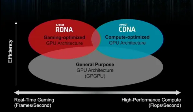
- GPU: parallel compute units often require many blocks to run concurrently, resulting in high power—some SoCs disable or omit GPUs to save power;
- Memory: main memories such as DDR consume significant power as they are frequently accessed.
Other modules may also consume power, but clock tree, CPU/GPU, and memory typically dominate. In AI accelerators, interconnect and on-chip network (CCN) IP can be a major power source similar to GPU fabrics.
Conclusion
Low-power techniques are essential knowledge for SoC design. Without an understanding of these techniques, it is difficult to follow design choices and trade-offs across a project or to participate effectively in technical discussions.