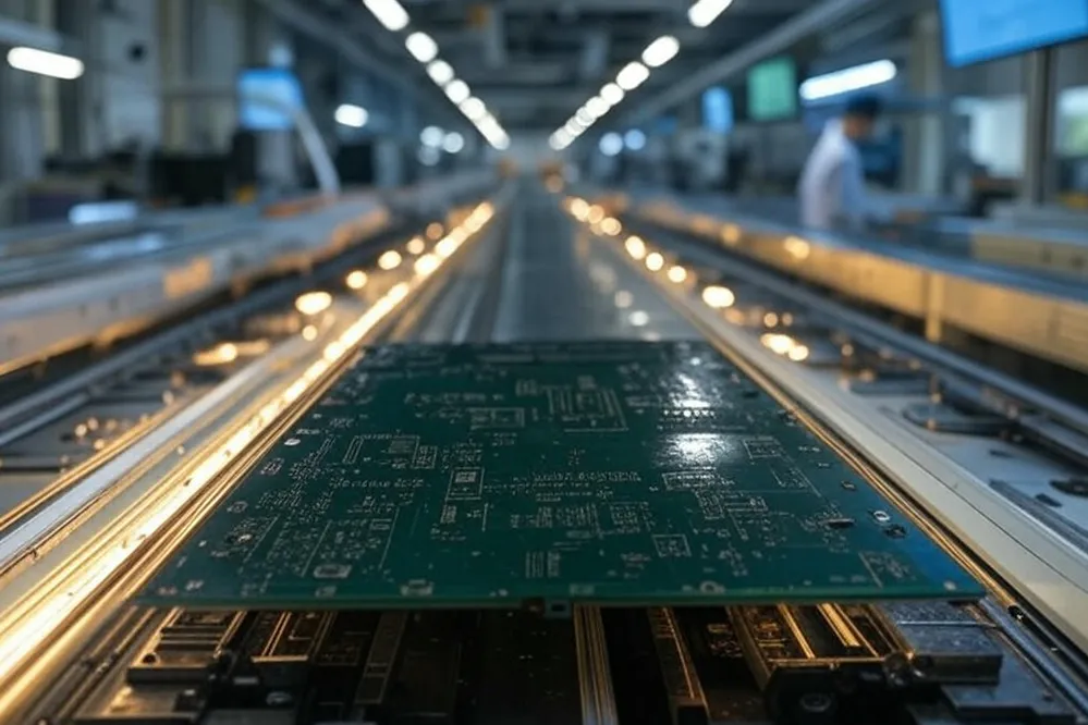
ALLPCB


PCB Advanced Options
When you try to submit a new order, there might be some options different from the normal process, how do you indicate it when placing an order?
In ALLPCB we sort these as advanced options, today we gonna introduce to you what they are and how to choose the special options you need for your project.
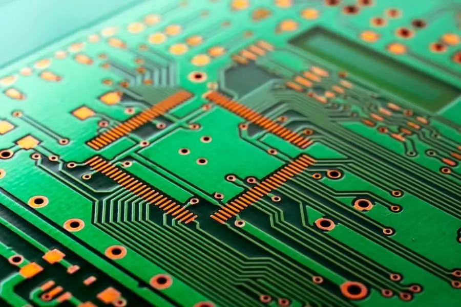
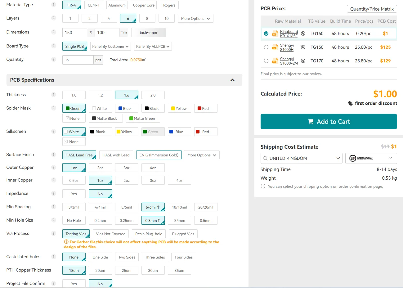
After you fill in the PCB Specifications, you will notice a folded section at the bottom of the page called "Advanced options". When you open this section, you will find there many options, which is the topic we are going to discuss today.
Due to the special nature of these processes, manual pricing is still required. After you select the relevant items and submit them, our colleagues who are responsible for pricing will evaluate the cost and manufacturing time based on the actual details of your Gerber files. So, typically, after you select the relevant items, the price displayed at that moment is not the final price. We will inform you of the final price after confirming the pricing.
Let's go ahead and start introducing these topics then!
Edge Plating
In PCB manufacturing, side plating—also known as Castellation or Edge plating—refers to the process of metalizing the edges of a circuit board. Specifically, it involves applying copper plating along the edges, extending from the top to the bottom surface of the board. The surface treatment for side plating can include ENIG, ENEPIG, HASL, or other treatments that ensure electrical connectivity. Side plating enables the use of the PCB's edges for technical features during subsequent assembly. Both the PCB's outline and certain interior areas can be metalized.
Carbon Ink
Carbon ink on a PCB is a type of conductive ink that contains carbon particles. It's typically used to create resistive traces or to provide additional conductivity in certain areas of the circuit board. Carbon oil board is a relatively common surface treatment method for single and double-side PCBs. Through a series of inspections, tests and aging tests, and other technical processes, the PCB can work reliably for a long time.
Carbon ink can be applied in various ways, such as screen printing, to form patterns on the PCB. It's often used for creating features like printed resistors, touch-sensitive areas, or grounding planes. The ink offers a relatively low-cost and flexible solution compared to traditional copper traces, and it can also be used for protective or aesthetic purposes.
Serial Number
A serial number on a PCB is a unique identifier assigned to each board during production. It helps track and trace each PCB throughout its lifecycle, from manufacturing to testing and shipping. The serial number can be used for purposes such as quality control, warranty management, or identifying specific batches of PCBs.
Typically, serial numbers are printed on the PCB surface using methods like laser marking or ink printing, and they can be located in non-critical areas to avoid interference with the circuit's functionality. This unique identifier ensures that any issues can be traced back to the specific board, and it also helps with inventory and logistics management.
Blue Glue
Peelable solder mask on a PCB is a temporary coating applied to specific areas of the board that need to remain protected during certain stages of the manufacturing process. It acts as a protective layer that can be easily removed (peeled off) after the soldering process, leaving the PCB ready for final assembly.
This type of solder mask is commonly used to protect pads or areas where components will be soldered later, preventing contamination or accidental solder bridging during previous manufacturing steps. Once the PCB goes through soldering or wave soldering, the peelable mask can be removed to reveal the clean, ready-to-use pads or surfaces. It provides a cost-effective way to ensure clean, reliable soldering without damaging the PCB.
Countersink Hole/Step Hole
A Countersink Hole is a hole that has been drilled with a conical shape at the top, designed to allow a countersunk screw or another fastener to sit flush with or below the surface of the PCB. The countersink feature creates a space for the head of a screw to fit into, allowing it to be recessed or sunk below the board's surface. This type of hole is typically used to secure components or for mechanical purposes like attaching the PCB to a chassis.
Further reading: Understanding Countersink Holes in PCB Design
Press-fit hole
A press-fit hole on a PCB is a type of hole designed to accommodate components that are pressed into place without the need for soldering. These components, often connectors or pins, have a special design that allows them to be mechanically inserted into the hole and securely held by friction. The press-fit technology ensures a reliable electrical and mechanical connection.
The press-fit holes typically have precise tolerances(ALLPCB standard:±0.05mm) and are plated with copper to ensure proper conductivity. This method is commonly used in high-reliability applications, such as in aerospace or automotive industries, where a strong, durable connection is needed. It also eliminates the need for soldering, which can reduce the risk of thermal damage and improve the overall robustness of the PCB.
CTI≥600V
CTI (Comparative Tracking Index) ≥ 600V refers to the electrical property of a PCB material that indicates its resistance to tracking, which is the formation of conductive paths on the surface of the material due to electrical stress and contamination. The CTI value measures the voltage at which this tracking occurs. A CTI ≥ 600V means the PCB material is highly resistant to electrical tracking and can safely withstand voltages of 600 volts or higher without the risk of surface degradation or electrical short circuits caused by tracking.
This property is especially important in environments with high voltage or potential for contamination (such as moisture or dust), where tracking could lead to failures or safety hazards. PCBs with a CTI ≥ 600V are typically used in applications requiring high reliability and electrical safety, such as in industrial, automotive, or aerospace electronics.
Chamfering/Beveling
In the printed circuit board industry, chamfering and beveling are two widely used techniques for modifying the edges of the board. Though these terms are sometimes used interchangeably, they refer to distinct processes with different purposes and results.Chamfering involves cutting or grinding a small portion of the board’s edge at a 45-degree angle. This creates a beveled edge that is smoother and less prone to catching on other materials or objects. Chamfering is commonly applied to PCB corners to prevent damage during handling or installation and can also be used for aesthetic purposes, providing a more polished or finished look.Beveling, on the other hand, involves removing a larger portion of the edge at an angle other than 45 degrees, resulting in a sloped edge. Beveling is often used to fit the PCB into a specific shape or housing, reduce the board's overall size while preserving functionality, or create a more aerodynamic design, especially in applications like drones or UAV electronics.