 ALLPCB


In today’s world, sustainability is no longer just a buzzword—it’s a necessity. For engineers working on printed circuit board (PCB) design, creating products that are easy to disassemble and recycle is becoming a critical skill. If you’re searching for practical ways to implement design for disassembly PCB, follow PCB recycling guidelines, or create a recyclable PCB design, this guide is for you. We’ll walk you through the principles of eco-design PCB and DFD PCB (Design for Disassembly) to help you build sustainable electronics that reduce e-waste and support a circular economy.
This comprehensive blog post dives deep into actionable strategies, technical considerations, and best practices for designing PCBs with disassembly and recycling in mind. Whether you’re a seasoned engineer or just starting out, you’ll find valuable insights to make your designs more environmentally friendly.
Why Design for Disassembly and Recycling Matters in PCB Engineering
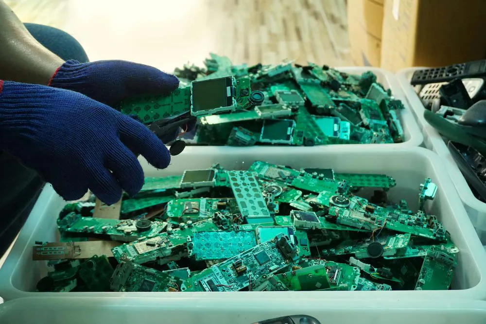
The electronics industry produces millions of tons of e-waste every year. According to the Global E-waste Monitor, over 53 million metric tons of electronic waste were generated worldwide in 2019, and this number is growing. PCBs, as the backbone of most electronic devices, contribute significantly to this problem due to their complex composition of metals, plastics, and hazardous materials like lead or brominated flame retardants.
Designing PCBs for disassembly and recycling—often referred to as DFD PCB—helps address these challenges by making it easier to recover valuable materials, reduce landfill waste, and minimize environmental harm. Beyond environmental benefits, adopting eco-design PCB principles can also lower production costs over time, improve brand reputation, and ensure compliance with increasingly strict regulations on e-waste management.
What Are the Core Goals of Design for Disassembly (DFD) in PCBs?
The main idea behind design for disassembly PCB is to create boards that can be taken apart easily at the end of their lifecycle. This involves:
- Simplifying the separation of components for reuse or recycling.
- Minimizing the use of hazardous materials that complicate recycling processes.
- Maximizing the recovery of valuable metals like gold, silver, and copper, which can make up 30-50% of a PCB’s weight, as noted in recent studies on e-waste composition.
Key Principles of Recyclable PCB Design
Creating a recyclable PCB design requires careful planning from the earliest stages of development. Below are the core principles to guide your work as an engineer.
1. Material Selection for Sustainability
The materials you choose for your PCB play a huge role in its recyclability. Traditional PCBs often use substrates and components that are hard to separate or contain toxic substances. To align with eco-design PCB goals, consider the following:
- Use Lead-Free Solder: Lead is a hazardous material that poses risks during recycling. Opt for lead-free alternatives like tin-silver-copper (SAC) alloys, which are widely accepted and safer for the environment.
- Avoid Brominated Flame Retardants: These chemicals, often used in PCB laminates, can release toxic fumes when processed. Look for halogen-free materials that meet fire safety standards without compromising recyclability.
- Choose Recyclable Substrates: Standard FR-4 substrates are common, but they’re often mixed with non-recyclable resins. Explore bio-based or recyclable laminate options where possible.
By prioritizing sustainable materials, you make the recycling process more efficient and reduce the environmental footprint of your design.
2. Modular Design for Easy Disassembly
One of the cornerstones of design for disassembly PCB is modularity. A modular PCB is built in a way that allows components to be removed or replaced without damaging the board or surrounding parts. Here’s how to achieve this:
- Use Connectors Instead of Soldering: Where feasible, use plug-in connectors for major components rather than permanent soldering. This makes it easier to detach parts like microcontrollers or power modules during disassembly.
- Group Similar Components: Place components with similar recycling processes (e.g., all capacitors or resistors) in clusters. This simplifies sorting during recycling.
- Minimize Adhesives: Avoid glues or adhesives that bond components permanently to the board, as they make separation difficult.
3. Reduce Component Complexity
Complex designs with densely packed components or multi-layer boards can be a nightmare to disassemble. To follow PCB recycling guidelines, aim for simplicity:
- Limit Layer Count: While multi-layer PCBs are often necessary for high-performance applications, try to minimize the number of layers. Fewer layers mean easier separation during recycling.
- Avoid Embedded Components: Components embedded within the board are nearly impossible to remove without destroying the PCB. Keep components surface-mounted whenever possible.
- Standardize Parts: Use standard, widely available components rather than custom or proprietary ones. This makes replacement and recycling more straightforward.
Practical PCB Recycling Guidelines for Engineers
Beyond design choices, engineers must understand the recycling process to make informed decisions. Here are practical PCB recycling guidelines to keep in mind while designing.
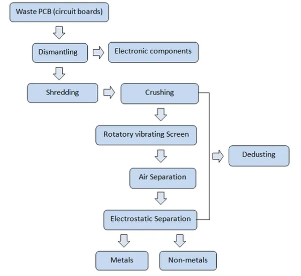
1. Understand the Recycling Process
PCB recycling typically involves several stages: disassembly, shredding, and material recovery (through physical, thermal, or chemical methods). Knowing this can shape how you design. For instance:
- During shredding, mixed materials can contaminate valuable metals. Designing with uniform material types in mind helps improve recovery rates.
- Chemical recovery often targets precious metals like gold and silver. Ensure these are accessible by avoiding coatings or laminates that hinder extraction.
2. Label Components Clearly
Clear labeling is a simple yet powerful step in recyclable PCB design. Mark components with their material composition or recycling codes. This helps recycling facilities identify and sort parts quickly, reducing contamination risks. For example, label plastic connectors with their resin identification codes (similar to those used in packaging) to streamline processing.
3. Design with End-of-Life in Mind
Always ask yourself: “How will this PCB be handled when it’s no longer in use?” Designing with the end-of-life stage in mind ensures that your board doesn’t end up as landfill waste. This ties directly into DFD PCB principles, focusing on ease of separation and material recovery.
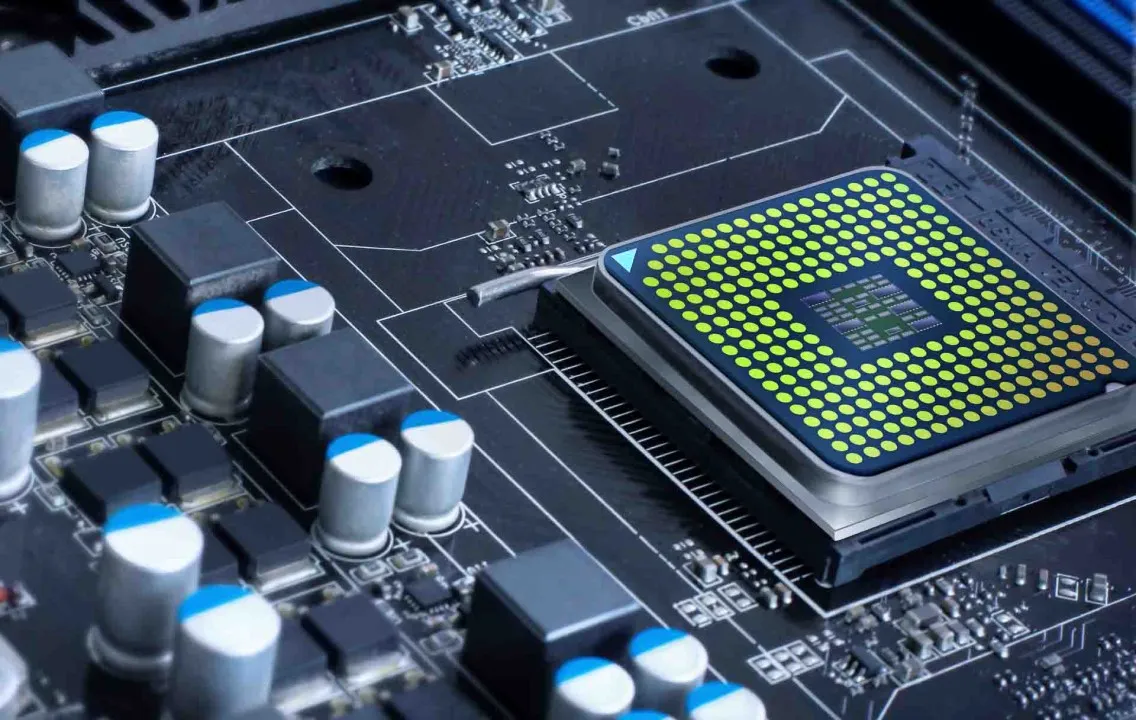
Technical Considerations for Eco-Design PCB
While sustainability is the goal, engineers must balance it with performance. Here are some technical considerations to ensure your eco-design PCB meets both environmental and functional needs.
1. Maintain Signal Integrity in Simplified Designs
Simplifying a PCB for disassembly can sometimes risk signal integrity, especially in high-speed applications. For instance, reducing layer count might increase crosstalk or impedance mismatch. To counter this:
- Keep critical signal traces on outer layers for easier access and better control of impedance (typically targeting values like 50 ohms for high-speed signals).
- Use ground planes strategically to minimize interference, even in designs with fewer layers.
2. Optimize for Thermal Management
Eco-friendly materials like halogen-free laminates may have different thermal properties than traditional options. Ensure your design accounts for heat dissipation, especially in power-intensive applications. For example, place high-heat components near thermal vias or heat sinks, and test for operating temperatures (often aiming for under 85°C for most components) to prevent failures.
3. Test for Durability During Disassembly
A PCB designed for disassembly must still withstand the process without breaking apart prematurely. Use simulation tools to test mechanical stress points, ensuring that connectors or modular sections can be removed without damaging traces or substrates.
Benefits of Adopting DFD PCB and Eco-Design Practices
Investing time and effort into design for disassembly PCB and eco-design PCB offers several advantages for engineers and manufacturers:
- Cost Savings: Recovering materials like copper (which can constitute up to 20% of a PCB’s weight) reduces the need for raw material purchases.
- Regulatory Compliance: Many regions, like the European Union, enforce strict e-waste laws under directives like WEEE (Waste Electrical and Electronic Equipment). Designing for recycling helps meet these standards.
- Brand Reputation: Companies that prioritize sustainability often gain consumer trust and loyalty, especially as environmental awareness grows.
Challenges in Implementing Recyclable PCB Design
While the benefits are clear, there are hurdles to overcome when adopting recyclable PCB design practices:
- Higher Initial Costs: Sustainable materials or modular designs may cost more upfront, though they often pay off in the long term.
- Performance Trade-Offs: Simplifying designs or using alternative materials can sometimes impact speed or reliability, requiring careful testing.
- Limited Industry Standards: Unlike traditional PCB design, there are fewer universally accepted guidelines for DFD or recycling-focused designs, making it a learning curve for many engineers.
Steps to Start Designing Sustainable PCBs Today
Ready to integrate PCB recycling guidelines and DFD PCB principles into your workflow? Follow these actionable steps:
- Assess Your Current Designs: Review your existing PCB layouts for areas where disassembly or material choices can be improved.
- Research Sustainable Materials: Look for suppliers offering lead-free, halogen-free, or bio-based options for substrates and components.
- Collaborate with Recycling Experts: Partner with recycling facilities to understand their processes and challenges, tailoring your designs to their needs.
- Use Design Tools: Leverage PCB design software with features for modularity and material tracking to streamline your eco-design efforts.
- Test and Iterate: Build prototypes of your recyclable designs, test them for performance and disassembly, and refine based on results.
Conclusion: Building a Sustainable Future with Eco-Design PCB
As engineers, we have the power to shape a more sustainable future through thoughtful design. By embracing design for disassembly PCB, adhering to PCB recycling guidelines, and prioritizing recyclable PCB design, we can reduce e-waste, recover valuable resources, and protect the environment. The journey toward eco-design PCB and DFD PCB practices may come with challenges, but the long-term benefits—for the planet, for businesses, and for innovation—are undeniable.
Start small by incorporating one or two of the strategies discussed in this guide into your next project. Over time, these efforts will compound, contributing to a circular economy where electronics are no longer a burden but a resource. Let’s design not just for today, but for generations to come.


