ALLPCB


If you're looking to understand the multi-layer PCB manufacturing process, you've come to the right place. Multi-layer PCBs (Printed Circuit Boards) are essential for complex electronics, offering compact designs with multiple layers of conductive material. In this guide, we'll walk you through the detailed, step-by-step process of manufacturing these boards, from initial design to final testing. Whether you're an engineer, designer, or hobbyist, this comprehensive overview will help you grasp the intricacies of creating high-quality multi-layer PCBs for your projects.
What Is a Multi-Layer PCB?
A multi-layer PCB is a type of circuit board that has more than two layers of conductive material, typically copper, separated by insulating layers. These boards are used in advanced electronics like smartphones, medical devices, and industrial equipment because they allow for higher circuit density and better performance in a smaller space. Unlike single or double-layer boards, multi-layer PCBs can have anywhere from 4 to over 20 layers, depending on the complexity of the design.
Understanding how these boards are made is key to ensuring they meet the strict requirements of modern technology. Let’s dive into the step-by-step process of multi-layer PCB manufacturing.
Why Choose Multi-Layer PCBs?
Before we explore the manufacturing process, it’s worth noting why multi-layer PCBs are so popular. They offer several advantages:
- Compact Design: Multiple layers allow for more components in a smaller footprint, ideal for portable devices.
- Improved Signal Integrity: With dedicated ground and power planes, these boards reduce noise and interference, supporting high-speed signals (often above 1 GHz in modern applications).
- Enhanced Durability: The layered structure adds strength and resistance to environmental factors.
- Flexibility: They can handle complex circuits with thousands of connections, which single-layer boards cannot support.
Now, let’s break down the manufacturing process to see how these benefits are achieved through precise engineering.
The Multi-Layer PCB Manufacturing Process: Step by Step
Creating a multi-layer PCB is a complex, multi-stage process that requires precision at every step. Below, we outline the key stages involved in transforming a design into a functional board.
Step 1: Design and Schematic Creation
The journey begins with the design phase. Engineers use specialized software to create a schematic diagram that outlines the circuit’s layout and connections. This schematic serves as the blueprint for the PCB, detailing where each component will go and how the layers will interconnect.
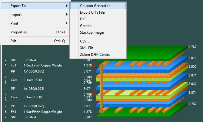
During this stage, designers also define the stack-up, which is the arrangement of conductive and insulating layers. For instance, a 6-layer PCB might have two signal layers on the outside, with ground and power planes in the middle, separated by insulating material. Impedance control is critical here, often targeting values like 50 ohms for high-speed signals to prevent signal loss.
Step 2: Design Validation and Gerber File Generation
Once the design is complete, it undergoes validation to check for errors like short circuits or incorrect component placements. After validation, the design is exported into Gerber files, which are industry-standard formats used to communicate the layout to manufacturers. These files include details for each layer, drill holes, and other specifications.
Accuracy at this stage is crucial. Even a small error in the Gerber files can lead to costly mistakes during production, such as misaligned vias or incorrect copper traces.
Step 3: Material Selection and Preparation
Multi-layer PCBs are made from a combination of conductive and insulating materials. The core material is often FR-4, a type of fiberglass epoxy laminate, while copper foil is used for conductive layers. The thickness of the copper can vary, typically ranging from 1 oz (35 micrometers) to 2 oz (70 micrometers) per square foot, depending on current-carrying needs.
Materials are cut to size and cleaned to remove any contaminants that could affect adhesion or conductivity during later steps. Prepreg, a semi-cured resin material, is also prepared to bond the layers together.
Step 4: Inner Layer Imaging and Etching
For multi-layer boards, the inner layers are processed first. A photoresist layer is applied to the copper-clad core material, and the design for each inner layer is transferred using UV light exposure through a photomask. Areas exposed to light harden, while unexposed areas remain soft and are washed away, revealing the copper pattern beneath.
Next, the board undergoes etching, where a chemical solution removes the unwanted copper, leaving only the desired traces and pads. The remaining photoresist is then stripped away, and the inner layers are inspected for accuracy.
Step 5: Layer Alignment and Lamination
Once the inner layers are ready, they are stacked together with prepreg material between them to act as an insulator and adhesive. Alignment is critical, as even a misalignment of 0.1 mm can cause connection issues. Special alignment pins or optical systems ensure precision.
The stack is then placed in a lamination press, where heat (typically around 170-180°C) and pressure (up to 300 psi) are applied. This bonds the layers into a single, solid board. The prepreg cures during this process, creating a strong, unified structure.
Step 6: Drilling Vias and Through-Holes
After lamination, holes are drilled into the board for vias (connections between layers) and through-holes (for component leads). High-speed CNC drilling machines are used, capable of creating holes as small as 0.2 mm in diameter. The placement and size of these holes are guided by the Gerber files to ensure accuracy.
Drilling generates heat and debris, so the board is cleaned afterward to remove burrs and residue that could affect conductivity.
Step 7: Plating and Copper Deposition
To connect the layers electrically, the drilled holes are plated with copper. This process, known as electroless copper deposition, creates a thin conductive layer inside the holes. Then, electroplating thickens the copper to ensure reliable connections, often achieving a thickness of 25-30 micrometers.
This step is vital for ensuring that signals can travel between layers without interruption, especially in high-frequency applications where resistance must be minimized.
Step 8: Outer Layer Imaging and Etching
Similar to the inner layers, the outer layers are coated with photoresist, exposed to UV light through a mask, and developed to reveal the circuit pattern. Etching removes the unwanted copper, leaving the final traces and pads on the surface. These outer layers often include component mounting areas and signal routing.
Inspection follows to ensure there are no defects like over-etching or incomplete traces that could affect functionality.
Step 9: Solder Mask Application
A solder mask, usually green but available in other colors, is applied to the board to protect the copper traces from oxidation and prevent short circuits during assembly. The mask is applied as a liquid or film, exposed to UV light to harden it, and then developed to expose areas for soldering, such as pads and vias.
The solder mask also improves the board’s appearance and durability, protecting it from environmental factors like moisture and dust.
Step 10: Silkscreen Printing
A silkscreen layer is added to label components, test points, and other important markers on the board. This is typically done with white ink, though other colors can be used. The silkscreen helps during assembly and troubleshooting by providing clear visual guides.
Precision is important here to ensure markings are legible and correctly placed, especially on densely populated boards.
Step 11: Surface Finish Application
A surface finish is applied to the exposed copper areas to prevent oxidation and enhance solderability. Common finishes include HASL (Hot Air Solder Leveling), ENIG (Electroless Nickel Immersion Gold), and OSP (Organic Solderability Preservative). For high-reliability applications like aerospace, ENIG is often preferred due to its durability and flat surface, ideal for fine-pitch components.
The choice of finish impacts the board’s performance and cost, so it’s selected based on the project’s needs.
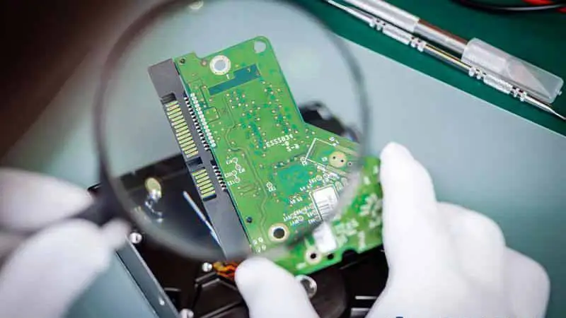
Step 12: Electrical Testing
Before the board is considered complete, it undergoes electrical testing to verify connectivity and detect defects like open circuits or shorts. Techniques like flying probe testing or bed-of-nails testing are used, checking for continuity and insulation resistance across all layers.
For multi-layer boards, testing is especially critical due to the complexity of internal connections. A failure rate of even 1% can be costly in high-volume production.
Step 13: Final Inspection and Quality Control
A final visual and automated optical inspection (AOI) is conducted to check for surface defects, misalignments, or other issues. Dimensional accuracy is verified to ensure the board matches the design specifications, often within tolerances of ±0.05 mm for critical features.
Quality control at this stage ensures that only defect-free boards move on to assembly or shipping.
Step 14: Panel Separation and Packaging
Multi-layer PCBs are often manufactured in panels containing multiple boards to improve efficiency. After testing, individual boards are separated from the panel using routing or scoring techniques. Edges are smoothed to prevent damage during handling.
The boards are then packaged with protective materials to avoid scratches or static damage during transport.
Step 15: Assembly (Optional)
While not always part of the manufacturing process, many projects move directly to assembly after fabrication. Components are placed and soldered onto the board using automated pick-and-place machines and reflow soldering. For multi-layer boards, this step requires precision to handle dense layouts and fine-pitch components.
Post-assembly testing ensures the board functions as intended before it’s integrated into the final product.
Key Considerations in Multi-Layer PCB Manufacturing
Manufacturing multi-layer PCBs involves several challenges that must be addressed to ensure quality:
- Layer Alignment: Misalignment can cause connection failures, so precision tools are essential.
- Thermal Management: High-density designs generate heat, requiring careful material selection and layout planning.
- Signal Integrity: Maintaining impedance (often 50-100 ohms for RF applications) and minimizing crosstalk are critical for performance.
- Cost Control: More layers mean higher costs, so designs must balance complexity with budget constraints.
Working with experienced manufacturers can help navigate these challenges and deliver reliable boards for any application.
Conclusion
Multi-layer PCB manufacturing is a detailed and precise process that transforms complex designs into functional circuit boards. From initial design and material selection to lamination, drilling, and testing, each step plays a vital role in ensuring the final product meets the demands of modern electronics. By understanding this process, engineers and designers can make informed decisions to optimize performance, reduce costs, and achieve high-quality results.
At ALLPCB, we’re committed to providing top-tier manufacturing services to bring your multi-layer PCB designs to life. Whether you’re working on a prototype or high-volume production, our expertise ensures precision and reliability at every stage. Dive into the world of advanced electronics with confidence, knowing that the foundation of your project is built to last.