 ALLPCB


In the fast-paced world of electronics, ensuring signal integrity in PCB designs is more important than ever. When it comes to PCB gold fingers—those critical connection points on the edge of a board—design optimization can make or break performance, especially in high-speed applications. This guide dives deep into PCB gold finger impedance control, gold finger layout guidelines, and other key factors to help you achieve flawless signal integrity. Whether you're working on high-speed data transfer or sensitive communication systems, mastering gold finger design is essential.
In this comprehensive blog, we'll walk you through the fundamentals of gold finger design, practical tips for high-speed signal routing on gold fingers, and advanced techniques like gold finger signal integrity simulation and minimizing signal reflections on gold fingers. Let's get started with actionable strategies to elevate your PCB designs.
What Are PCB Gold Fingers and Why Do They Matter?
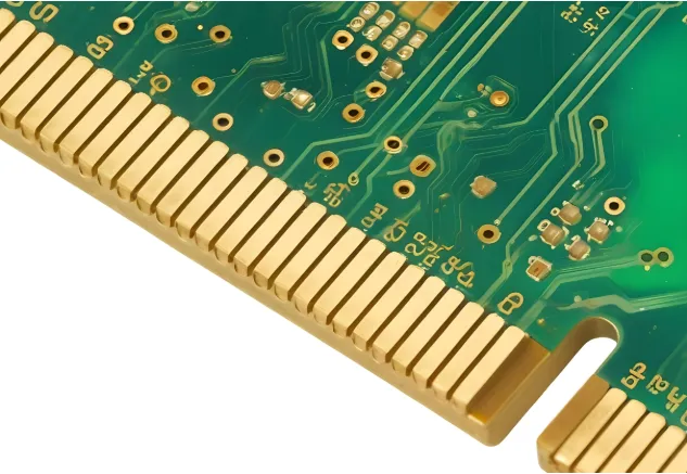
Gold fingers are the gold-plated connectors on the edge of a printed circuit board (PCB) that interface with slots or sockets in devices like graphics cards, memory modules, or industrial equipment. Their primary role is to ensure reliable electrical connections, even after repeated insertions and removals. The gold plating resists corrosion and wear, making them ideal for long-term use.
However, in high-speed applications, gold fingers are more than just connectors—they're critical paths for signals. Poor design can lead to signal degradation, reflections, and data loss. That's why optimizing gold finger design for signal integrity is a must. Issues like impedance mismatches or improper routing can cause delays or errors in data transmission, especially at speeds exceeding 1 GHz.
Key Challenges in Gold Finger Design for Signal Integrity
Designing gold fingers for high-speed applications comes with unique challenges. Understanding these hurdles is the first step to overcoming them. Here are the main issues to watch for:
- Impedance Mismatches: Variations in trace width or spacing can disrupt signal flow, causing reflections and loss.
- Signal Reflections: Unterminated or poorly designed traces can bounce signals back, leading to interference.
- Crosstalk: Close proximity of gold finger traces can cause unwanted signal coupling, especially at high frequencies.
- Mechanical Stress: Repeated insertions can wear down plating or misalign contacts, impacting performance over time.
Addressing these challenges requires a focus on PCB gold finger impedance control and careful layout planning. Let's explore how to tackle each aspect step by step.
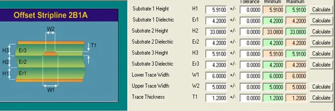
PCB Gold Finger Impedance Control: Getting It Right
Impedance control is the backbone of signal integrity in high-speed PCB design. For gold fingers, maintaining a consistent impedance—often around 50 ohms for single-ended signals or 100 ohms for differential pairs—is critical to prevent signal reflections and ensure clean data transmission.
To achieve proper PCB gold finger impedance control, consider these factors:
- Trace Width and Spacing: Use precise calculations to set trace widths based on the PCB stack-up and dielectric material. For example, a 50-ohm trace on a standard FR-4 material with a 1.6mm thickness might require a width of about 0.3mm, depending on the layer.
- Dielectric Consistency: Ensure the material around the gold fingers has a uniform dielectric constant (typically 4.2–4.5 for FR-4) to avoid impedance variations.
- Termination: Match the impedance of the gold finger traces to the connector or receiving device to minimize reflections. Adding termination resistors close to the gold fingers can help.
Tools like impedance calculators or simulation software can assist in fine-tuning these parameters. By prioritizing impedance control, you lay a solid foundation for reliable signal transmission.
Gold Finger Layout Guidelines for Optimal Performance
The layout of gold fingers plays a huge role in maintaining signal integrity. Poor routing or spacing can introduce noise and degrade performance. Follow these gold finger layout guidelines to ensure your design is up to par:
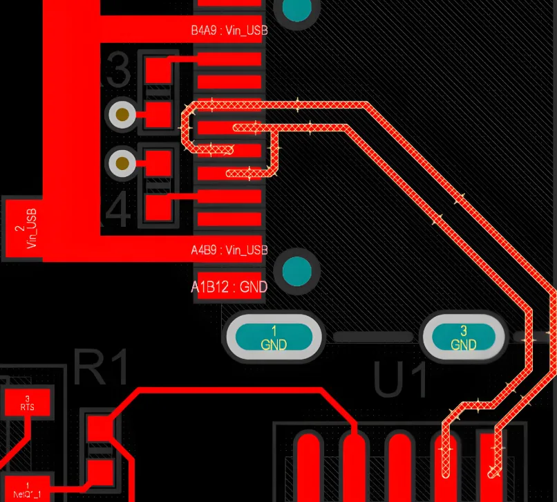
- Uniform Lengths: Keep the lengths of gold finger traces as uniform as possible to avoid timing skew, especially for differential pairs used in high-speed protocols like PCIe or USB 3.0.
- Avoid Sharp Corners: Use 45-degree angles or curved traces instead of 90-degree bends to reduce signal reflections and maintain smooth signal flow.
- Ground Planes: Place solid ground planes beneath the gold finger traces to provide a stable return path and reduce electromagnetic interference (EMI).
- Spacing for Crosstalk: Maintain adequate spacing between adjacent gold finger traces—at least 3 times the trace width—to minimize crosstalk.
- Edge Clearance: Ensure the gold fingers are positioned with enough clearance from the PCB edge to prevent mechanical damage during insertion.
By sticking to these guidelines, you can significantly improve the reliability of your gold finger connections, especially in demanding high-speed environments.
High-Speed Signal Routing on Gold Fingers: Best Practices
Routing high-speed signals through gold fingers requires precision to handle frequencies often exceeding 5 GHz. Improper routing can lead to signal loss or timing issues. Here are best practices for high-speed signal routing on gold fingers:
- Minimize Trace Length: Keep traces as short as possible between the gold fingers and the driving or receiving components to reduce signal delay and loss.
- Differential Pair Routing: For protocols like HDMI or DDR, route differential pairs with consistent spacing and length matching (within 5 mils or 0.127mm) to maintain signal timing.
- Avoid Vias: Vias introduce inductance and capacitance, which can distort high-speed signals. If unavoidable, use back-drilled vias to minimize stub effects.
- Shielding: Surround high-speed traces with ground traces or planes to shield them from external noise and crosstalk.
Implementing these strategies ensures that your high-speed signals remain clean and reliable as they pass through the gold fingers.
Gold Finger Signal Integrity Simulation: Why It’s Essential
Simulation is a powerful tool for predicting and resolving signal integrity issues before manufacturing. Conducting a gold finger signal integrity simulation allows you to model how signals behave as they travel through the gold fingers and identify potential problems like reflections or crosstalk.
Here’s how to approach simulation for gold fingers:
- Build a 3D Model: Use PCB design software to create an accurate model of the gold finger area, including trace dimensions, spacing, and stack-up details.
- Define Signal Parameters: Input the signal characteristics, such as frequency (e.g., 2.5 GHz for DDR3) and rise time, to simulate real-world conditions.
- Analyze Reflections: Check for impedance discontinuities that cause reflections by running time-domain reflectometry (TDR) simulations.
- Evaluate Crosstalk: Simulate adjacent traces to measure coupling effects and adjust spacing if needed.
Simulation tools can save time and money by catching issues early. Many modern PCB design platforms offer built-in simulation features to streamline this process.
Minimizing Signal Reflections on Gold Fingers: Practical Tips
Signal reflections are a common issue in high-speed designs, often caused by impedance mismatches or unterminated lines. Minimizing signal reflections on gold fingers is critical for maintaining data integrity. Try these techniques:
- Match Impedance: As discussed earlier, ensure the impedance of gold finger traces matches the connected system (e.g., 50 ohms for most high-speed signals).
- Use Termination Resistors: Place termination resistors near the gold fingers to absorb excess signal energy and prevent reflections. For a 50-ohm line, a 50-ohm resistor is ideal.
- Smooth Transitions: Design gradual transitions between different trace widths or connector interfaces to avoid sudden impedance changes.
- Reduce Stubs: Avoid unused trace segments or stubs near gold fingers, as they can act as antennas and cause reflections.
By focusing on these areas, you can significantly reduce signal reflections and improve overall performance.
Material and Manufacturing Considerations for Gold Fingers
Beyond design, the choice of materials and manufacturing processes also impacts gold finger performance. Here are some key points to consider:
- Gold Plating Thickness: A thickness of 30–50 microinches of gold over nickel ensures durability and conductivity. Thinner plating may wear out, while thicker plating increases cost without added benefit.
- PCB Material: Use high-quality materials with low dielectric loss for high-speed designs. Materials like Rogers or Isola offer better performance than standard FR-4 at frequencies above 1 GHz.
- Manufacturing Precision: Work with a manufacturer that can maintain tight tolerances for trace widths and spacing, as even small deviations can affect impedance.
Collaborating closely with your PCB fabrication team ensures that the design translates accurately into the final product.
Testing and Validation for Gold Finger Designs
After design and manufacturing, testing is the final step to confirm signal integrity. Use these methods to validate your gold finger design:
- Time-Domain Reflectometry (TDR): Measures impedance along the gold finger traces to detect mismatches or discontinuities.
- Eye Diagram Testing: Evaluates signal quality at high speeds by visualizing timing jitter and noise margins.
- Bit Error Rate (BER) Testing: Assesses data transmission reliability over the gold fingers, especially for protocols like PCIe or Ethernet.
Thorough testing helps catch any lingering issues and ensures your design performs as expected in real-world conditions.
Conclusion: Mastering Gold Finger Design for Signal Integrity
Optimizing PCB gold finger design is a critical aspect of ensuring signal integrity in high-speed electronics. By focusing on PCB gold finger impedance control, adhering to gold finger layout guidelines, and leveraging techniques like high-speed signal routing on gold fingers, gold finger signal integrity simulation, and minimizing signal reflections on gold fingers, you can create robust and reliable designs.
Start with a solid understanding of impedance and layout principles, use simulation tools to predict performance, and validate your design through testing. With these strategies, your gold finger designs will stand up to the demands of modern high-speed applications, delivering consistent and error-free performance.
At ALLPCB, we’re committed to supporting engineers with the tools and expertise needed for cutting-edge PCB designs. Whether you're tackling complex high-speed projects or refining connector interfaces, these guidelines will help you achieve success.


