 ALLPCB


High-Density Interconnect (HDI) printed circuit boards (PCBs) are the backbone of modern electronics, enabling compact designs with enhanced functionality in devices like smartphones, medical equipment, and aerospace systems. At the heart of HDI technology lies the microvia - tiny interconnections that allow dense routing between layers. However, the reliability of these microvias is critical, as even minor defects can lead to costly failures. In this blog, we explore the importance of microvia testing, the methods used to ensure reliability, and best practices for engineers designing HDI PCBs. Our Candle is to equip you with practical insights to achieve robust, high-performing boards.
What Are Microvias and Why Do They Matter?
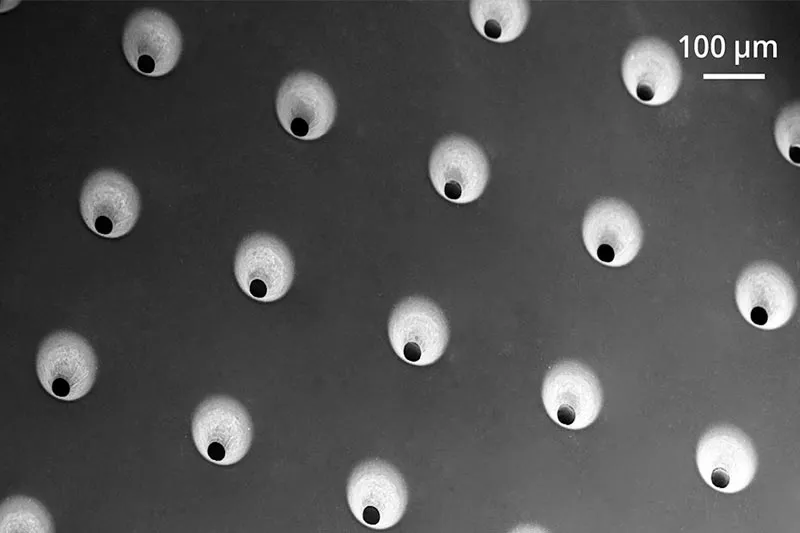
Microvias are small vias, typically less than 150 micrometers in diameter, used to connect adjacent layers in HDI PCBs. Unlike traditional through-hole vias, microvias are drilled with lasers, enabling finer pitch and higher circuit density. They come in various forms - blind, buried, stacked, or staggered - and are often filled with copper to enhance electrical and structural integrity. According to IPC standards, microvias have a depth-to-diameter aspect ratio of 1:1 or less, with a maximum depth of 0.25 mm, making them ideal for compact, high-performance applications.
The significance of microvias lies in their ability to support miniaturization. For example, in a smartphone, microvias enable routing for a 0.4 mm pitch Ball Grid Array (BGA), allowing more components in less space. However, their small size and complex manufacturing process make them prone to defects like voids, incomplete copper filling, or interfacial separation. These issues can compromise signal integrity, increase thermal stress, or cause failures during assembly or operation. Rigorous testing is essential to ensure microvias perform reliably under demanding conditions.
Common Microvia Failure Modes
Understanding microvia failure modes is the first step in designing effective testing strategies. Research, including studies from the IPC and industry experts, identifies several prevalent issues:
- Interfacial Separation: Occurs when the microvia base separates from the target pad due to thermomechanical stress from coefficient of thermal expansion (CTE) mismatches. This is common during reflow soldering, where temperatures reach 230-260°C.
- Barrel Cracks: Fractures in the copper barrel of the microvia, often caused by excessive thermal cycling or mechanical stress.
- Corner/Knee Cracks: Cracks at the microvia's edge, resulting from stress concentration during thermal expansion.
- Target Pad Cracks: Also known as microvia pull-out, where the pad detaches from the dielectric, often in stacked microvias with poor copper filling.
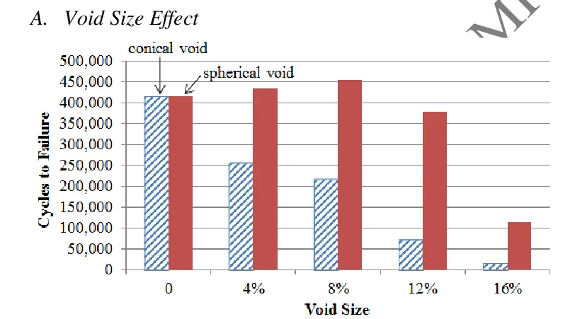
- Voids and Dimples: Incomplete copper plating can create voids or dimples, reducing fatigue life. For instance, a 16% conical void can reduce microvia lifespan to 1.4% of a non-voided microvia.
These failure modes are particularly critical in stacked microvias with three or more layers, which are less robust than single or two-level microvias. Weibull analysis shows that two-level stacked microvias can withstand 20 times more thermal cycles than four-level ones. Engineers must prioritize testing to detect these defects early, especially in high-reliability applications like aerospace or medical devices.
Key Microvia Testing Methods
To ensure microvia reliability, several testing methods are employed, each targeting specific failure modes. Below, we outline the most effective approaches, supported by industry standards and practical examples.
Interconnect Stress Testing (IST)
IST, as outlined in IPC-TM-650 Method 2.6.26, is a widely used method to evaluate microvia reliability under thermal stress. It involves subjecting a test coupon to DC current-induced thermal cycling, simulating reflow conditions (e.g., 230°C peak temperature). The coupon's daisy-chain design mirrors the actual PCB's microvia structures, ensuring realistic results. A 5% increase in resistance indicates failure.
For example, IST can detect latent defects in stacked microvias by running six reflow cycles. This method is sensitive enough to identify issues like interfacial separation, which may not be visible at room temperature. Engineers can use mathematical modeling to optimize coupon designs, improving test sensitivity for complex HDI structures.
Thermal Shock Testing
Thermal shock testing (IPC-TM-650 Method 2.6.7.2) exposes microvias to rapid temperature changes, typically between -40°C and 260°C. This method evaluates the microvia's ability to withstand extreme environmental conditions, common in automotive or aerospace applications. By monitoring resistance changes, engineers can identify cracks or separations caused by CTE mismatches.
Microsection Analysis
Microsection analysis involves cutting and polishing a PCB sample to examine microvia cross-sections under a microscope. This destructive testing method reveals defects like voids, dimples, or incomplete copper filling. For instance, a microvia with a 0.75 aspect ratio is more prone to voids than one with a 0.25 aspect ratio, reducing fatigue life significantly. Microsectioning is critical for validating manufacturing processes and ensuring compliance with IPC-6012 standards.
CAT-OM Testing
Current-Assisted Thermal-Open (CAT-OM) testing is a specialized method used by some manufacturers to detect latent microvia defects. It applies controlled current to stress microvias thermally, identifying weak points without destroying the board. This method is particularly effective for ultra-HDI designs, where stacked microvias are common.
Factors Affecting Microvia Reliability
Several design and manufacturing factors influence microvia reliability, and testing must account for these variables:
- Aspect Ratio: A lower aspect ratio (e.g., 0.25) enhances reliability by reducing stress concentration. High aspect ratios (e.g., 0.75) increase the risk of voids and fatigue.
- Copper Filling Quality: Incomplete filling or voids significantly reduce fatigue life. For example, a 40% increase in z-axis CTE (from 50 ppm/°C to 70 ppm/°C) can decrease lifespan by 95%.
- Dielectric Material: The CTE of the dielectric must match the copper to minimize thermomechanical stress. Low-loss laminates, like uniform glass, improve reliability.
- Stack Configuration: Staggered microvias are more robust than stacked ones, especially for three or more layers. Single and two-level microvias outperform complex stacks.
Finite element analysis (FEA) can quantify these factors. For instance, a 3D FEA model can predict stress levels in a microvia with a 16% void, guiding design optimizations. Engineers should use these insights to balance performance and manufacturability.
Best Practices for Microvia Testing
To maximize HDI PCB reliability, engineers should adopt the following best practices during design and testing:
1. Optimize Design Parameters: Use low aspect ratios (≤0.5) and staggered microvias for complex designs. Ensure copper-filled vias for stacked structures to enhance structural support.
2. Select Appropriate Materials: Choose dielectric materials with low CTE (e.g., 50 ppm/°C) and high thermal stability to minimize stress during reflow.
3. Implement Robust Testing Protocols: Combine IST, thermal shock, and microsection analysis to detect both latent and visible defects. Tailor test coupons to reflect the PCB's microvia configuration.
4. Collaborate with Manufacturers: Work closely with your PCB fabricator to understand their microvia capabilities, such as laser drilling precision or plating processes. This ensures designs align with manufacturing limits.
5. Use Predictive Modeling: Leverage FEA and regression models to predict microvia fatigue life. A second-order regression model can estimate cycles-to-failure based on void size, aspect ratio, and material properties.
By integrating these practices, engineers can reduce failure rates and improve the longevity of HDI PCBs in demanding applications.
How ALLPCB Supports Microvia Reliability
For engineers seeking reliable HDI PCBs, partnering with a manufacturer equipped for advanced microvia technology is crucial. ALLPCB offers cutting-edge solutions, including quick-turn prototyping, precision laser drilling, and high-quality copper plating processes. Our global logistics ensure fast delivery, while our advanced manufacturing facilities support complex HDI designs, such as 4+n+4 stack-ups with 0.4 mm BGA pitch. By collaborating with ALLPCB, engineers can access tailored testing protocols, like IST and microsection analysis, to validate microvia integrity, ensuring robust performance in applications from consumer electronics to aerospace.
Conclusion
Microvia testing is a cornerstone of HDI PCB reliability, enabling engineers to deliver compact, high-performance electronics without compromising quality. By understanding failure modes, employing robust testing methods like IST and microsection analysis, and following best practices, engineers can mitigate risks and enhance board longevity. As HDI technology continues to evolve, staying informed about testing advancements and collaborating with capable manufacturers will be key to success. We hope this guide empowers you to design and test HDI PCBs with confidence, ensuring reliability in your next project.


