ALLPCB


If you're looking to enhance the quality of solder joints in PCB wave soldering, you've come to the right place. This guide offers a clear, step-by-step approach to tackle common challenges like poor solderability, inconsistent wetting, and weak joints. We'll dive into optimizing factors such as PCB wave soldering solderability, wetting angle, intermetallic compound formation, surface tension, and inspection techniques to ensure reliable results for your printed circuit boards.
Wave soldering is a widely used method for assembling through-hole components on PCBs, but achieving consistent, high-quality solder joints requires attention to detail. From preparing the board to fine-tuning the soldering process, this blog will walk you through practical solutions to improve outcomes and reduce defects. Let's explore how to elevate your PCB manufacturing process.
What is Wave Soldering and Why Does Solder Joint Quality Matter?
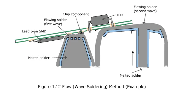
Wave soldering is a bulk soldering process used to attach through-hole components to a PCB. The board passes over a molten solder wave, which coats the exposed metal areas and forms connections between components and the board. This method is efficient for high-volume production but can lead to issues like incomplete wetting, solder bridging, or weak joints if not done correctly.
Solder joint quality directly impacts the reliability and performance of electronic devices. Poor joints can cause electrical failures, reduced mechanical strength, or long-term reliability issues due to thermal cycling or vibration. By focusing on key aspects like PCB wave soldering solderability and inspection, manufacturers can minimize defects and ensure durable connections. In this post, we'll break down actionable steps to achieve that.
Step 1: Optimize PCB Design for Wave Soldering Solderability
The foundation of high-quality solder joints starts with the PCB design. PCB wave soldering solderability refers to how well the board's surface and components accept solder. Poor solderability often leads to incomplete joints or defects like solder skips.
To improve solderability, ensure that the PCB surface finish is compatible with wave soldering. Common finishes like HASL (Hot Air Solder Leveling) provide a thin layer of solder on pads, enhancing solderability by protecting the underlying copper from oxidation. Avoid finishes prone to oxidation if delays occur between manufacturing and assembly. Additionally, ensure pad sizes are adequate—typically 1.5 to 2 times the diameter of the component lead—to allow proper solder flow.
Component placement also plays a role. Arrange components to minimize shadowing, where taller components block the solder wave from reaching nearby pads. Orient components perpendicular to the direction of the wave to ensure even solder distribution. By focusing on these design elements, you can significantly boost PCB wave soldering solderability and set the stage for strong joints.
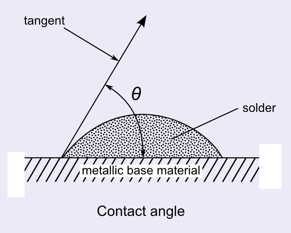
Step 2: Control the Wetting Angle for Better Solder Joints
The wetting angle in PCB wave soldering is the angle formed between the solder and the surface of the pad or component lead. A smaller wetting angle (ideally less than 30 degrees) indicates good wetting, meaning the solder spreads evenly and bonds well. A larger angle (above 90 degrees) suggests poor wetting, often resulting in weak or incomplete joints.
To achieve an optimal PCB wave soldering wetting angle, start by ensuring clean surfaces. Contaminants like oxides or residues on pads and leads can prevent proper wetting. Use a pre-fluxing step before soldering to remove oxides and promote adhesion. Fluxes with higher activity levels, such as rosin-based or water-soluble fluxes, are often effective for wave soldering.
Temperature control is also critical. The solder wave temperature should typically be set between 250°C and 260°C for standard tin-lead solder, or around 260°C to 270°C for lead-free solder. If the temperature is too low, the solder may not wet properly; if too high, it can damage components or the board. Monitor the conveyor speed as well—speeds between 1.5 to 2.5 meters per minute allow sufficient contact time with the wave for proper wetting without excess heat exposure.
Step 3: Manage Intermetallic Compound Formation
During soldering, an intermetallic compound (IMC) forms at the interface between the solder and the base metal, usually copper. In PCB wave soldering, intermetallic compound layers like Cu6Sn5 and Cu3Sn are essential for a strong bond, as they indicate proper metallurgical bonding. However, excessive IMC growth can make joints brittle and prone to cracking under stress.
To manage PCB wave soldering intermetallic compound formation, control the soldering temperature and duration of contact with the molten solder. Prolonged exposure to high temperatures (above 260°C for more than 5-10 seconds) can accelerate IMC growth. Adjust the conveyor speed to limit contact time with the solder wave to 2-4 seconds for most applications.
The choice of solder alloy also influences IMC formation. Lead-free solders like SAC305 (Sn-3.0Ag-0.5Cu) tend to form thicker IMC layers compared to traditional tin-lead solders due to higher tin content. If reliability is a concern, consider testing different alloys to balance IMC growth with joint strength. Regular monitoring of the solder bath for impurities, such as copper or iron buildup, can also prevent excessive IMC formation by maintaining solder purity.
Step 4: Understand and Adjust Surface Tension in Wave Soldering
Surface tension in PCB wave soldering refers to the force that affects how molten solder flows and adheres to surfaces. High surface tension can cause the solder to bead up rather than spread evenly, leading to poor wetting and incomplete joints. Low surface tension, on the other hand, may result in solder bridging between closely spaced pads.
To optimize PCB wave soldering surface tension, flux plays a crucial role. Flux reduces surface tension by breaking down oxides and allowing solder to flow more freely across pads and leads. Ensure the flux is evenly applied using a foam or spray method before the board reaches the solder wave. Insufficient flux can lead to high surface tension and poor wetting, while excess flux can leave residues that affect long-term reliability.
The design of the solder wave itself also matters. Modern wave soldering machines often use dual-wave systems—a turbulent wave for initial contact and a smooth laminar wave for finishing. The turbulent wave helps penetrate tight spaces and reduce surface tension effects, while the laminar wave ensures a clean finish. Adjust wave height to ensure full contact with the board, typically 2-3 mm above the board surface, to achieve consistent results.
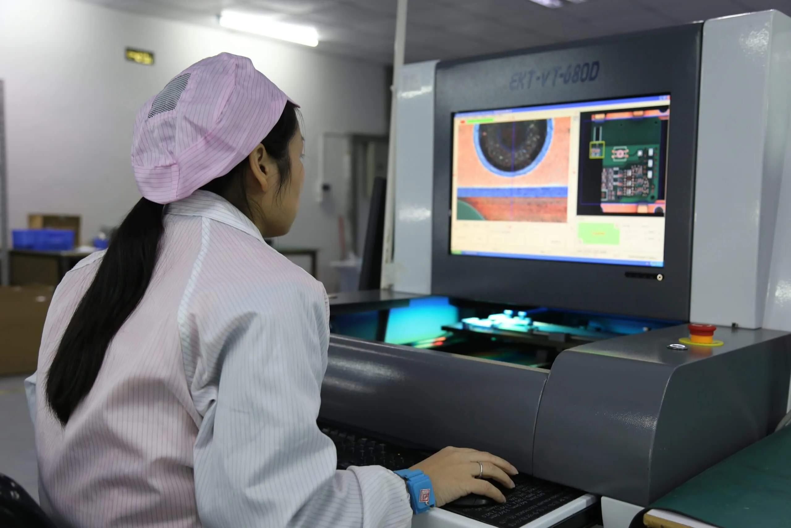
Step 5: Implement Effective Inspection Techniques
Inspection is a vital step to ensure solder joint quality in PCB wave soldering. PCB wave soldering inspection helps identify defects like insufficient solder, bridging, or poor wetting before they lead to failures in the field. A combination of visual and automated inspection methods can provide comprehensive quality control.
Start with visual inspection under magnification (10x to 20x) to check for obvious issues. Look for shiny, smooth solder joints that fully cover pads and leads, indicating good wetting. Dull or grainy joints may suggest contamination or poor temperature control. Check for solder bridges between adjacent pads, which often result from excess solder or improper wave height.
For more detailed analysis, use Automated Optical Inspection (AOI) systems. AOI can detect defects like solder skips or insufficient fillet height with high precision, scanning entire boards in seconds. Set AOI parameters to flag joints with fillet heights less than 0.5 mm or wetting angles greater than 60 degrees as potential issues. For critical applications, X-ray inspection can reveal hidden defects, such as voids within solder joints, which may weaken mechanical strength.
Finally, consider periodic solderability testing of incoming PCBs and components using methods like the dip-and-look test or wetting balance test. These tests measure how well solder adheres to surfaces, helping identify potential issues before production. By integrating these PCB wave soldering inspection techniques, you can catch and correct problems early, ensuring consistent quality.
Step 6: Fine-Tune Process Parameters for Consistency
Consistency in wave soldering comes from tightly controlled process parameters. Beyond temperature and conveyor speed, monitor the solder bath composition. For lead-free solders, maintain tin content within ±0.5% of the specified alloy (e.g., 96.5% for SAC305) to prevent variations in melting point or wetting behavior. Regularly skim dross—oxidized solder—from the bath surface to avoid contamination, ideally every 4-8 hours of operation.
Preheat temperature is another key factor. Set the preheater to 100°C-120°C for most PCBs to reduce thermal shock when the board contacts the solder wave. This helps maintain even wetting and prevents component damage. Use thermal profiling tools to measure the actual temperature across the board during preheating and soldering, ensuring no cold spots compromise joint quality.
Lastly, maintain equipment regularly. Clean flux applicators daily to prevent uneven coating, and check wave uniformity to avoid areas of low solder flow. Small adjustments, like ensuring the wave height remains within 0.5 mm of the target, can make a big difference in achieving uniform solder joints across large production runs.
Step 7: Address Common Defects and Their Root Causes
Even with optimized processes, defects can occur. Understanding their causes helps in troubleshooting. Solder bridging, for instance, often results from excessive solder wave height or high surface tension. Reduce wave height or adjust flux application to mitigate this. Insufficient solder, on the other hand, may stem from poor PCB wave soldering solderability due to oxidized pads—ensure proper storage conditions (humidity below 50%) for boards before assembly.
Solder skips, where the wave misses certain pads, can occur due to shadowing or low wave height. Reorient components or increase wave height slightly to resolve this. Voids within joints, visible via X-ray, may indicate trapped flux or moisture. Extend preheat time to 60-90 seconds to evaporate moisture before soldering.
Track defect rates over time to identify patterns. If bridging occurs in 5% or more of boards, for example, it’s a sign to recalibrate wave parameters. Keeping a log of defects and adjustments helps refine the process continuously.
Conclusion: Building Reliability Through Better Wave Soldering
Improving solder joint quality in PCB wave soldering is a multi-step process that demands attention to design, materials, equipment settings, and inspection. By focusing on aspects like PCB wave soldering solderability, wetting angle, intermetallic compound management, surface tension, and thorough inspection, you can achieve strong, reliable joints that stand up to the demands of modern electronics.
Start with a well-designed PCB and clean, compatible materials. Fine-tune your soldering parameters—temperature, speed, and wave height—to ensure consistent wetting and minimal defects. Use robust inspection methods to catch issues early, and continuously monitor and adjust your process for long-term success. With these steps, you’ll not only reduce rework but also deliver high-quality boards that meet industry standards.
At ALLPCB, we’re committed to supporting your manufacturing journey with resources and expertise to optimize every stage of PCB assembly. Implement these strategies in your wave soldering process, and watch your solder joint quality reach new heights.