 ALLPCB


In the world of high-speed PCB design, maintaining signal integrity is crucial for ensuring reliable performance. One key factor that directly affects signal integrity is trace spacing. But how does maximum trace spacing impact signal integrity? Simply put, trace spacing influences crosstalk, impedance control, and overall signal quality in a printed circuit board (PCB). When traces are spaced too closely, interference and noise can degrade signals, while excessive spacing can lead to layout inefficiencies and other design challenges.
In this comprehensive guide, we’ll dive deep into the relationship between trace spacing and signal integrity, exploring its effects on PCB crosstalk, impedance control, and high-speed PCB design. Whether you’re an experienced engineer or just starting out, this blog will provide actionable insights to help you optimize your designs for better performance.
Understanding Trace Spacing in PCB Design
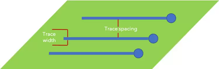
Trace spacing refers to the distance between two conductive traces on a PCB. These traces carry electrical signals between components, and their spacing plays a critical role in how those signals behave. In high-speed PCB design, where signals switch at frequencies above 100 MHz, even small variations in trace spacing can cause significant issues.
The primary goal of managing trace spacing is to minimize interference while maintaining a compact and efficient layout. If traces are too close, electromagnetic fields from one trace can interfere with another, leading to a phenomenon called crosstalk. On the other hand, spacing traces too far apart can increase the board size unnecessarily, raising costs and complicating routing.
Signal Integrity: The Foundation of Reliable PCB Performance
Signal integrity refers to the quality of an electrical signal as it travels through a PCB. A signal with good integrity maintains its shape, timing, and amplitude without distortion or noise. Poor signal integrity can result in data errors, timing issues, and system failures, especially in high-speed applications like USB, HDMI, or DDR memory interfaces.
Several factors affect signal integrity, including trace length, impedance mismatches, and electromagnetic interference (EMI). Trace spacing is particularly important because it directly impacts crosstalk and impedance control—two critical elements in high-speed designs.
How Trace Spacing Affects Crosstalk in PCBs
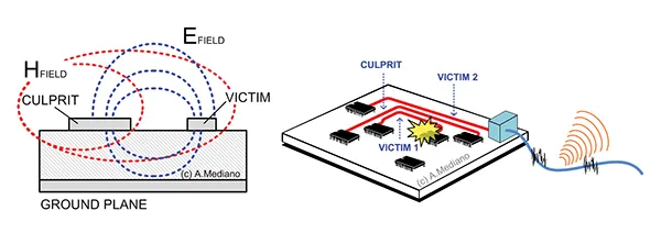
Crosstalk occurs when a signal on one trace induces an unwanted signal on a nearby trace due to electromagnetic coupling. This interference can corrupt data and degrade performance, especially in high-speed circuits. The closer the traces, the stronger the coupling, and the higher the risk of crosstalk.
For example, in a design with parallel traces running at 1 GHz, reducing the spacing from 10 mils (0.254 mm) to 5 mils (0.127 mm) can increase crosstalk by up to 20-30%, depending on the dielectric material and trace length. To mitigate this, designers often follow the "3W rule," which suggests that the spacing between traces should be at least three times the width of the trace to reduce crosstalk to acceptable levels.
However, maximum trace spacing isn’t always the solution. While increasing spacing reduces crosstalk, it can lead to larger board sizes and routing challenges. Striking a balance is key, and simulation tools can help predict crosstalk levels based on specific spacing values.
Trace Spacing and Impedance Control: A Critical Connection
Impedance control is another vital aspect of high-speed PCB design, ensuring that signals travel without reflections or losses. The characteristic impedance of a trace depends on its width, thickness, spacing to adjacent traces or planes, and the dielectric constant of the board material. For high-speed signals like those in USB 3.0 (5 Gbps), maintaining a consistent impedance—often 50 ohms for single-ended signals or 100 ohms for differential pairs—is essential.
Trace spacing impacts impedance, especially in differential pair routing. If the spacing between the two traces in a differential pair is too large, the impedance increases, leading to mismatches that cause signal reflections. For instance, a differential pair with a target impedance of 100 ohms might require a spacing of 8 mils (0.203 mm) on a standard FR-4 material with a dielectric constant of 4.2. Increasing the spacing to 12 mils (0.305 mm) could raise the impedance to 110 ohms, introducing reflections and degrading signal integrity.
Designers must use impedance calculators or simulation software to determine the optimal trace spacing for their specific stack-up and signal requirements. Layer stack-up design also plays a role, as spacing to reference planes (ground or power) affects impedance alongside trace-to-trace spacing.
Challenges of Maximum Trace Spacing in High-Speed PCB Design
While increasing trace spacing can reduce crosstalk and help with impedance control, pushing spacing to the maximum isn’t always practical or beneficial. Here are some challenges associated with maximum trace spacing in high-speed PCB design:
- Increased Board Size: Wider spacing means traces take up more real estate, leading to larger boards. This can increase manufacturing costs and may not be feasible for compact devices like smartphones or IoT modules.
- Routing Complexity: High-speed designs often involve dense component placement. Excessive spacing can make it harder to route traces efficiently, especially in multi-layer boards with limited space.
- Signal Timing Issues: In differential pairs or matched-length traces, excessive spacing can introduce skew—where one signal arrives slightly before the other—causing timing errors. For example, at 10 Gbps, a 1 mil (0.0254 mm) length mismatch due to spacing can result in a timing skew of about 6 picoseconds, which is significant for such high speeds.
Designers must weigh these trade-offs when deciding on trace spacing. Often, a middle ground—balancing spacing for signal integrity with practical layout constraints—is the best approach.
Best Practices for Optimizing Trace Spacing in High-Speed Designs
To achieve optimal signal integrity while managing trace spacing, consider the following best practices tailored for high-speed PCB design:
- Follow Industry Guidelines: Use established rules like the 3W rule for spacing to minimize crosstalk. For differential pairs, adhere to spacing recommendations based on target impedance (e.g., 8-10 mils for 100-ohm differential impedance on FR-4).
- Use Simulation Tools: Leverage PCB design software with built-in signal integrity analysis to simulate crosstalk and impedance based on trace spacing. Adjust spacing iteratively to find the sweet spot for your design.
- Prioritize Ground Planes: A solid ground plane beneath signal traces can reduce crosstalk by providing a return path for electromagnetic fields. Keep spacing between signal layers and ground planes consistent to maintain impedance.
- Route High-Speed Signals First: Plan the routing of critical high-speed signals before other traces to ensure adequate spacing and minimize interference. Group similar signals together while maintaining spacing to avoid coupling.
- Consider Material Properties: The dielectric constant (Dk) of your PCB material affects both impedance and crosstalk. For high-speed designs, low-Dk materials like Rogers or Isola can allow tighter spacing without sacrificing signal integrity.
Real-World Applications: Trace Spacing in Action
Let’s look at a practical example to see how trace spacing impacts signal integrity in real-world scenarios. Consider a PCB designed for a 5G communication module operating at 3.5 GHz. At such high frequencies, signal integrity is paramount to avoid data loss or bit errors.
In this design, the critical traces are differential pairs for data transmission with a target impedance of 100 ohms. Using a standard 4-layer stack-up on FR-4 material, the optimal trace width is calculated as 6 mils (0.152 mm), with a spacing of 8 mils (0.203 mm) between the pair. Spacing to adjacent traces is set at 18 mils (0.457 mm) to follow the 3W rule (3 times the trace width). Simulation results show that crosstalk is below -30 dB, and impedance remains within ±5% of the target, ensuring reliable performance.
If the spacing between the differential pair is increased to 12 mils (0.305 mm), the impedance rises to 108 ohms, causing reflections that degrade signal quality. Conversely, reducing spacing to adjacent traces to 10 mils (0.254 mm) increases crosstalk to -20 dB, introducing noise. This example highlights the delicate balance required in trace spacing for high-speed PCB design.
Advanced Techniques for Managing Trace Spacing
For complex designs, standard spacing rules may not be enough. Here are advanced techniques to further optimize trace spacing and signal integrity:
- Guard Traces: Place grounded traces between high-speed signal traces to act as shields, reducing crosstalk. Ensure these guard traces are connected to ground at multiple points for effectiveness.
- Staggered Routing: Avoid running parallel traces over long distances. Instead, stagger or cross traces at 90-degree angles to minimize coupling.
- Controlled Dielectric Thickness: Work with your manufacturer to control the dielectric thickness between layers, as this affects both impedance and crosstalk alongside trace spacing.
These techniques require careful planning and often collaboration with manufacturing partners to ensure feasibility and cost-effectiveness.
Conclusion: Striking the Right Balance with Trace Spacing
Trace spacing is a critical factor in maintaining signal integrity in high-speed PCB design. It directly impacts crosstalk, impedance control, and overall performance. While maximum trace spacing can reduce interference, it often comes with trade-offs like increased board size and routing challenges. By following best practices, leveraging simulation tools, and considering material properties, designers can optimize trace spacing to achieve reliable signal integrity without compromising on layout efficiency.
Understanding the relationship between trace spacing and signal integrity is essential for tackling the challenges of modern electronics, from 5G modules to high-speed data interfaces. With careful planning and the right design strategies, you can ensure your PCBs perform at their best, meeting the demands of today’s fast-paced technology landscape.


