 ALLPCB


Designing a printed circuit board (PCB) involves more than just electrical functionality; it also requires clear markings for assembly, testing, and troubleshooting. When it comes to the bottom layer of a PCB, silkscreen design plays a critical role in ensuring that markings are readable and effective. In this comprehensive guide, we’ll dive into PCB silkscreen design rules, focusing on bottom layer silkscreen guidelines, and cover essential aspects like silkscreen font size, silkscreen line width, and silkscreen spacing. Whether you're a seasoned engineer or new to PCB design, this post will provide actionable tips to achieve clarity and precision in your designs.
What Is PCB Silkscreen and Why Does It Matter for the Bottom Layer?
PCB silkscreen refers to the layer of text, symbols, and markings printed on the surface of a circuit board, typically using a non-conductive epoxy ink. These markings serve as a guide for component placement, polarity, and identification during assembly and maintenance. While the top layer often gets more attention due to its visibility, the bottom layer is equally important, especially for double-sided boards where components are mounted on both sides.
The bottom layer silkscreen must be designed with precision to avoid confusion during assembly or repair. Poorly designed markings—such as unreadable text or incorrect placement—can lead to costly errors, delays, or even board failures. By following proper bottom layer silkscreen guidelines, you ensure that your PCB remains functional and easy to work with throughout its lifecycle.
Key PCB Silkscreen Design Rules for the Bottom Layer
Designing silkscreen for the bottom layer requires attention to detail and adherence to specific rules. Below, we break down the most important PCB silkscreen design rules to help you create clear and effective markings.
1. Choose the Right Silkscreen Font Size for Readability
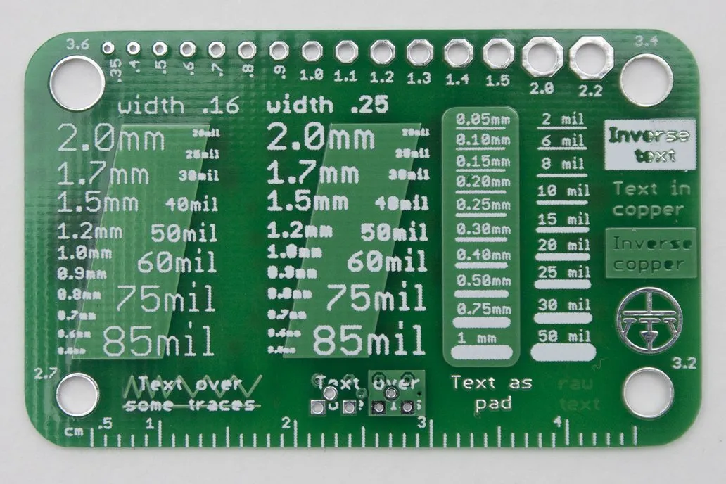
One of the most critical factors in silkscreen design is selecting an appropriate silkscreen font size. Text that is too small can be unreadable, while text that is too large may overcrowd the board and overlap with components or pads.
- Recommended Font Size: A minimum height of 50 mils (1.27 mm) for characters is widely recommended for readability by the naked eye. This ensures that assembly technicians and engineers can easily read component designators and labels.
- Bottom Layer Considerations: On the bottom layer, space is often limited due to component density. If 50 mils is not feasible, aim for a minimum of 40 mils (1.016 mm), but avoid going smaller as it risks becoming illegible.
Tip: Use vector-based fonts rather than raster fonts in your design software to maintain clarity during printing. Also, test the readability of your silkscreen by printing a sample or reviewing it at actual size on a monitor.
2. Maintain Proper Silkscreen Line Width for Clarity
The silkscreen line width refers to the thickness of the lines used to form text and symbols on the PCB. If the lines are too thin, they may not print clearly or could wear off over time. If they are too thick, they can make the text look cluttered or cause overlap.
- Minimum Line Width: A line width of at least 5 mils (0.127 mm) is a standard guideline in the industry. This thickness ensures that the silkscreen remains visible and durable during manufacturing and use.
- Bottom Layer Challenges: On the bottom layer, where space constraints are common, avoid increasing line width beyond 6-7 mils (0.152-0.178 mm) unless necessary, as it may cause text to merge or become unreadable.
Tip: Check with your PCB manufacturer for their specific capabilities, as some may have limitations or recommendations for line width based on their printing technology.
3. Optimize Silkscreen Spacing to Prevent Overlap
Proper silkscreen spacing is essential to prevent text and symbols from overlapping with components, pads, or other markings. Overcrowded silkscreen can lead to assembly errors or difficulty in identifying components.
- Minimum Spacing: Maintain a spacing of at least 6 mils (0.152 mm) between silkscreen elements and other board features like pads, vias, or component outlines. This prevents the silkscreen from interfering with soldering or component placement.
- Bottom Layer Focus: On the bottom layer, where components may be closely packed, ensure that silkscreen markings are placed outside the component footprint whenever possible. If space is tight, prioritize critical markings like polarity indicators over less essential labels.
Tip: Use design software tools to set up clearance rules for silkscreen layers, ensuring that spacing is automatically maintained during layout.
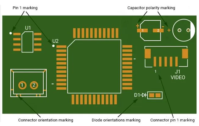
4. Ensure Uniform Orientation for Bottom Layer Markings
Consistency in the orientation of silkscreen text and symbols is crucial for readability. On the bottom layer, where the board may be flipped during assembly or inspection, maintaining a uniform reading direction is even more important.
- Standard Orientation: Align all text in a single direction, typically readable when the board is viewed with the bottom layer facing up. Avoid rotating text at odd angles unless necessary for specific components.
- Polarity and Pin Indicators: Clearly mark polarity for components like diodes and capacitors. Use standard symbols (e.g., a “+” for positive) and ensure they are positioned close to the relevant pad without overlapping.
Tip: If your design includes components with different orientations, group silkscreen text by section or area to minimize confusion.
5. Avoid Placing Silkscreen Over Pads and Vias
Silkscreen ink should never cover solder pads or vias, as it can interfere with soldering and electrical connections. This is especially critical on the bottom layer, where components are often soldered directly.
- Clearance Rule: Keep silkscreen markings at least 10 mils (0.254 mm) away from the edge of pads and vias. This clearance ensures that the ink does not affect the soldering process.
- Bottom Layer Priority: If space is limited, prioritize essential markings and omit non-critical text rather than risking overlap with pads or vias.
Tip: Use your PCB design software to run a design rule check (DRC) to identify any silkscreen violations before finalizing your layout.
Additional Bottom Layer Silkscreen Guidelines for Optimal Design
Beyond the core design rules, there are additional considerations specific to the bottom layer that can enhance the quality of your silkscreen markings.
1. Limit Silkscreen Density on the Bottom Layer
The bottom layer often has less available space due to component placement and routing. Overloading it with excessive silkscreen markings can create clutter and reduce readability.
- Prioritize Markings: Include only essential information, such as component designators, polarity indicators, and critical warnings. Omit non-essential logos or decorative elements if space is tight.
- Use Abbreviations: Where appropriate, use standard abbreviations (e.g., “R1” for resistor 1) to save space without sacrificing clarity.
2. Consider Silkscreen Color Contrast
While white and black are the most common silkscreen colors, the choice depends on the PCB’s solder mask color and the layer. On the bottom layer, ensure that the silkscreen color provides sufficient contrast against the background.
- Standard Practice: Use white silkscreen on a green or blue solder mask for better visibility. If the solder mask is a lighter color, consider black silkscreen ink.
- Bottom Layer Visibility: Since the bottom layer may be less accessible during inspection, high contrast is even more important to ensure quick identification of markings.
3. Test Silkscreen Placement During Prototyping
Before mass production, prototype your PCB to verify that the bottom layer silkscreen is clear and functional. Check for issues like text being obscured by components, insufficient spacing, or unreadable font sizes.
- Assembly Feedback: Work with your assembly team to confirm that the silkscreen aids in component placement and soldering without causing confusion.
- Iterative Improvement: Use feedback from the prototype stage to refine the silkscreen design for the final production run.
Common Mistakes to Avoid in Bottom Layer Silkscreen Design
Even with the best intentions, certain mistakes can compromise the effectiveness of your bottom layer silkscreen. Here are some pitfalls to watch out for:
- Ignoring Manufacturer Guidelines: Every PCB manufacturer may have specific requirements or limitations for silkscreen printing. Always review their design specifications to avoid issues during production.
- Overloading with Information: Too much text or too many symbols can clutter the bottom layer, making it difficult to read or use effectively.
- Inconsistent Markings: Mixing different font sizes, orientations, or styles can create a disorganized appearance and confuse assembly technicians.
Conclusion: Mastering Silkscreen Design for the Bottom Layer
Creating clear and effective silkscreen markings on the bottom layer of a PCB is a crucial step in ensuring a successful design. By following the PCB silkscreen design rules outlined in this guide—such as using an appropriate silkscreen font size of at least 50 mils, maintaining a silkscreen line width of 5 mils or more, and ensuring proper silkscreen spacing of at least 6 mils—you can avoid common errors and improve the usability of your board.
Paying attention to bottom layer silkscreen guidelines not only aids in assembly and troubleshooting but also enhances the overall quality of your PCB. Take the time to test your design during prototyping, prioritize essential markings, and collaborate with your manufacturing team to achieve the best results. With these practices in place, your PCB will be both functional and professional, meeting the needs of engineers and technicians alike.


