ALLPCB


In the fast-evolving world of unmanned aerial vehicles (UAVs), the performance of a drone often hinges on the quality of its printed circuit board (PCB) design. Poor signal integrity and electromagnetic interference (EMI) can lead to unreliable communication, erratic behavior, or even complete system failure. So, how do you ensure your UAV PCB operates at peak performance? By focusing on UAV PCB signal integrity optimization and implementing EMI reduction techniques for drone PCBs, you can create a robust design that withstands the challenges of high-speed signals and noisy environments.
In this comprehensive guide, we’ll dive into PCB layout guidelines for UAVs, explore signal integrity simulation for UAV PCB, and discuss effective UAV PCB grounding strategies. Whether you're an engineer designing cutting-edge drones or a hobbyist building a custom UAV, this blog will provide actionable insights to elevate your PCB design process.
Why Signal Integrity and EMI Matter in UAV PCB Design
Signal integrity refers to the quality of an electrical signal as it travels through a PCB. In UAVs, where high-speed data transmission is critical for real-time control, navigation, and communication, any signal distortion can lead to disastrous consequences. Similarly, EMI—unwanted electromagnetic noise—can interfere with sensitive components, disrupting the drone’s operation or causing it to lose connection with the controller.
Modern drones often operate at frequencies above 2.4 GHz for Wi-Fi or radio communication, and their compact designs pack multiple high-speed components into a small space. This combination increases the risk of crosstalk, signal delays, and EMI. By optimizing your PCB layout, you can minimize these risks and ensure reliable performance.
Key Principles of UAV PCB Signal Integrity Optimization
Optimizing signal integrity starts with understanding the factors that degrade signal quality, such as impedance mismatches, reflections, and crosstalk. Let’s break down actionable strategies to address these issues.
1. Control Impedance for High-Speed Signals
Impedance mismatches can cause signal reflections, leading to data errors. For UAV PCBs handling high-speed signals (like those for GPS or video streaming), maintaining consistent impedance is crucial. Aim for a standard impedance value, such as 50 ohms for RF traces or 100 ohms for differential pairs, depending on your design requirements.
Use trace width calculators to determine the correct dimensions based on your PCB stack-up and dielectric material. For example, a 4-layer PCB with a 1.6 mm thickness and FR-4 material might require a trace width of 0.3 mm for a 50-ohm impedance at 2.4 GHz. Additionally, avoid sharp bends in traces—use 45-degree angles or curved traces to minimize reflections.
2. Minimize Crosstalk Between Traces
Crosstalk occurs when signals on adjacent traces interfere with each other, a common issue in compact UAV designs. To reduce crosstalk, maintain a spacing of at least 3 times the trace width between high-speed signal lines. For instance, if your trace width is 0.2 mm, keep a 0.6 mm gap between parallel traces.
Routing differential pairs together with consistent spacing also helps. Place guard traces (grounded lines) between sensitive signals to act as a barrier against interference.
3. Shorten Trace Lengths for Critical Signals
Long traces increase the risk of signal delay and degradation. For time-critical signals like those used in flight control, keep trace lengths as short as possible. If a signal must travel a longer distance, use a higher layer count (e.g., 4 or 6 layers) to route signals more efficiently and avoid congestion on a single layer.
EMI Reduction Techniques for Drone PCBs
EMI can disrupt a drone’s communication systems or interfere with onboard sensors. Implementing effective EMI reduction techniques for drone PCBs is essential for reliable operation, especially in environments with high electromagnetic noise.
1. Use Proper Layer Stack-Up Design
A well-planned layer stack-up is one of the most effective ways to reduce EMI. For UAV PCBs, a 4-layer design is often ideal, with the following configuration:
- Top Layer: Signal traces and components
- Inner Layer 1: Ground plane
- Inner Layer 2: Power plane
- Bottom Layer: Additional signal traces or ground
The ground plane acts as a shield, reducing EMI by providing a low-impedance return path for signals. Ensure the ground plane is continuous, avoiding splits that can create loops and increase noise.
2. Add EMI Filters and Ferrite Beads
EMI filters and ferrite beads can suppress high-frequency noise on power lines. Place ferrite beads close to the power input of sensitive components like microcontrollers or RF modules. Pair them with bypass capacitors (e.g., 0.1 μF and 10 μF) to filter out a wide range of frequencies.
3. Shield Sensitive Components
For highly sensitive areas like RF circuits, consider using metal shields or cans. These enclosures block external EMI and prevent internal signals from radiating outward. Ensure the shield is properly grounded to avoid creating a floating conductor that could worsen interference.
PCB Layout Guidelines for UAVs
Following structured PCB layout guidelines for UAVs ensures that your design is both functional and reliable. Here are key practices to adopt.
1. Component Placement for Balance and Efficiency
In UAVs, weight distribution affects flight stability. Place heavier components, like power regulators or connectors, near the center of the PCB to maintain balance. Group related components (e.g., power supply circuits) together to minimize trace lengths and reduce noise.
Also, keep heat-generating components away from temperature-sensitive parts like sensors. Use thermal vias or heat sinks if needed to dissipate heat effectively.
2. Separate Analog and Digital Sections
Mixing analog and digital signals can lead to noise coupling. Designate separate areas on your PCB for analog components (like sensors) and digital components (like processors). Use a single ground plane but route return paths carefully to avoid overlap between analog and digital currents.
3. Optimize Power Distribution Network (PDN)
A stable power supply is critical for UAV performance. Place decoupling capacitors as close as possible to the power pins of ICs to filter out noise. For high-current components like motor controllers, use wider traces or power planes to handle the load without voltage drops.
Signal Integrity Simulation for UAV PCB
Before manufacturing your PCB, running a signal integrity simulation for UAV PCB can save time and costs by identifying potential issues early. Simulation tools allow you to analyze signal behavior, impedance, and crosstalk under real-world conditions.
1. Use Simulation Software for Pre-Layout Analysis
Start with pre-layout simulations to determine optimal trace widths, layer stack-ups, and component placements. Tools can model signal propagation at frequencies like 2.4 GHz, helping you spot reflections or delays before routing begins.
2. Post-Layout Verification
After completing your layout, perform post-layout simulations to verify signal integrity. Check for timing issues, voltage overshoots, or EMI hotspots. Adjust trace lengths or add termination resistors (e.g., 50 ohms for RF lines) if the simulation reveals problems.
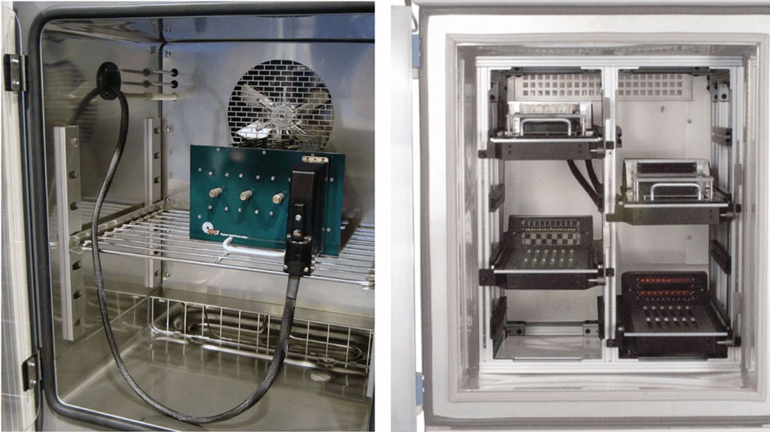
3. Thermal and EMI Simulations
Beyond signal integrity, simulate thermal performance to ensure components don’t overheat during flight. EMI simulations can also predict how your design will behave in noisy environments, allowing you to add filters or shields proactively.
UAV PCB Grounding Strategies
Effective UAV PCB grounding strategies are the foundation of both signal integrity and EMI reduction. A poor grounding scheme can turn your PCB into an antenna, radiating noise and disrupting performance.
1. Implement a Solid Ground Plane
A continuous ground plane provides a low-impedance path for return currents, reducing noise and EMI. Avoid splitting the ground plane unless absolutely necessary, as splits can create loops that amplify interference.
2. Use Star Grounding for Mixed Signals
In designs with both analog and digital signals, use a star grounding approach. Connect all ground points to a single central node to prevent noise from one section from affecting another. This method minimizes ground loops and ensures clean signal paths.
3. Ground Vias for Multi-Layer Boards
In multi-layer PCBs, place ground vias near high-speed signal transitions to provide a short return path. For example, add vias every 5-10 mm along a high-frequency trace to maintain signal integrity across layers.
Conclusion: Building Reliable UAV PCBs with Optimized Designs
Designing a UAV PCB that delivers excellent signal integrity and minimal EMI requires careful planning and attention to detail. By focusing on UAV PCB signal integrity optimization, applying EMI reduction techniques for drone PCBs, and following PCB layout guidelines for UAVs, you can create a board that performs reliably even in challenging conditions.
Start with a solid foundation—control impedance, minimize crosstalk, and use a proper layer stack-up. Leverage signal integrity simulation for UAV PCB to catch issues early, and adopt robust UAV PCB grounding strategies to eliminate noise. With these practices, your drone’s electronics will support seamless communication, precise control, and stable flight.
At ALLPCB, we’re committed to helping engineers and innovators bring their UAV designs to life with high-quality manufacturing and expert support. Whether you’re prototyping a new drone or scaling production, our services are tailored to meet your needs with precision and speed.