 ALLPCB


In the fast-paced world of fintech, where financial transactions happen in milliseconds, the reliability and efficiency of hardware are critical. Power Delivery Networks (PDN) in printed circuit boards (PCBs) play a vital role in ensuring stable power supply and minimizing noise for financial hardware. But how do you optimize a PDN for fintech PCBs to reduce noise and boost efficiency? The answer lies in careful design strategies like proper decoupling capacitor placement, maintaining power integrity, and using noise reduction techniques tailored for high-speed systems.
In this comprehensive guide, we’ll dive deep into PDN design for PCBs, focusing on power integrity in financial hardware. We’ll explore actionable noise reduction techniques for PCBs, the importance of decoupling capacitor placement, and effective voltage regulation in PCBs. Whether you’re an engineer designing fintech solutions or a hardware enthusiast, this blog will provide practical insights to enhance your PCB designs for optimal performance.
Why Power Delivery Networks Matter in Fintech PCBs
Fintech hardware, such as payment processing systems, high-frequency trading platforms, and cryptocurrency mining rigs, demands precision and speed. A poorly designed PDN can lead to voltage drops, electromagnetic interference (EMI), and signal integrity issues, all of which can cause transaction delays or data errors. In financial systems, even a microsecond of downtime can result in significant losses.
A well-optimized PDN ensures that power is delivered consistently across the PCB, maintaining stable voltage levels and minimizing noise. This is especially crucial in fintech, where components like microcontrollers, FPGAs, and ASICs require clean power to operate at peak efficiency. Let’s break down the key elements of PDN design for PCBs and how they apply to financial hardware.
Understanding PDN Design for PCBs: The Foundation of Power Integrity
PDN design for PCBs involves creating a network of components and traces that deliver power from the source to all parts of the board with minimal loss or interference. The goal is to achieve low impedance across a wide range of frequencies, ensuring that sudden current demands from components don’t cause voltage fluctuations.
In fintech hardware, where high-speed digital circuits are common, PDN design must account for dynamic loads. For instance, a high-frequency trading system might switch between idle and full processing modes in nanoseconds, creating rapid changes in current demand. If the PDN can’t respond quickly, voltage dips can occur, leading to errors. A target impedance of around 1 mΩ to 10 mΩ is often ideal for high-speed systems to keep voltage variations below 5% of the nominal value (e.g., 50 mV for a 1V rail).
Key aspects of PDN design include:
- Layer Stackup: Using dedicated power and ground planes to reduce impedance and provide a low-noise return path.
- Component Placement: Positioning power-hungry components close to voltage regulators to minimize trace length and resistance.
- Routing: Ensuring wide traces or planes for power delivery to handle high currents without significant voltage drops.
By focusing on these elements, engineers can build a robust PDN that supports the demanding requirements of financial hardware.
Power Integrity in Financial Hardware: Why It’s Non-Negotiable
Power integrity in financial hardware refers to the ability of the PDN to deliver clean, stable power under all operating conditions. Poor power integrity can lead to jitter in clock signals, data corruption, or even system crashes—issues that are unacceptable in fintech applications.
For example, in a payment processing terminal, power integrity ensures that the microprocessor handling encrypted transactions operates without glitches. A sudden voltage drop could corrupt data mid-transaction, leading to failed payments or security risks. Maintaining power integrity often involves a combination of proper PDN design, noise reduction techniques, and strategic component placement.
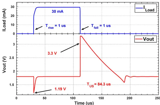
One critical metric for power integrity is the PDN’s ability to handle transient currents. High-speed fintech circuits might demand current spikes of several amperes in microseconds. If the PDN’s impedance is too high, these spikes cause voltage drops. Simulations and testing often aim for a transient response time of under 100 ns to keep up with these rapid changes.
Noise Reduction Techniques for PCBs: Keeping Fintech Systems Clean
Noise in PCBs can come from various sources, including switching regulators, high-speed digital signals, and external EMI. In fintech systems, noise can interfere with sensitive analog circuits or high-speed data lines, leading to errors. Here are some proven noise reduction techniques for PCBs:
1. Use of Ground Planes
A continuous ground plane provides a low-impedance return path for currents, reducing loop inductance and minimizing noise. Splitting ground planes should be avoided unless absolutely necessary for isolating analog and digital sections.
2. Filtering with Ferrite Beads
Ferrite beads, combined with capacitors, can filter out high-frequency noise from power lines. Placing a ferrite bead in series with the power supply line, followed by a 1 μF capacitor to ground, can suppress noise above 100 kHz.
3. Shielding Sensitive Areas
For fintech PCBs handling sensitive data, shielding critical components or traces with metal enclosures or guard rings can block external EMI. This is especially useful in environments with high electromagnetic activity, like data centers.
4. Minimize Crosstalk
Route high-speed traces away from power lines and use spacing or guard traces to prevent crosstalk. A spacing of at least 3x the trace width is often recommended for high-speed signals operating above 1 GHz.
By implementing these noise reduction techniques, engineers can ensure that fintech hardware operates reliably, even in noisy environments.
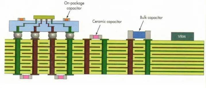
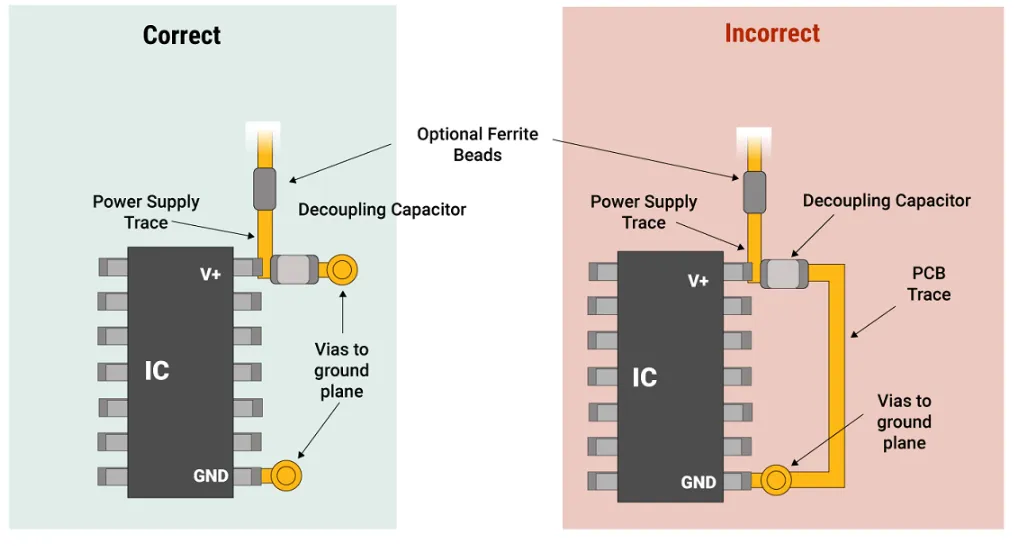
Decoupling Capacitor Placement: A Key to Stable Power Delivery
Decoupling capacitors are essential for stabilizing voltage and supplying instantaneous current to components during sudden load changes. In fintech PCBs, where high-speed processors and memory modules are common, proper decoupling capacitor placement can make or break the design.
The primary goal of decoupling capacitors is to act as local energy storage, reducing the impact of transient currents on the PDN. Here are some best practices for placement:
- Close Proximity: Place capacitors as close as possible to the power pins of ICs. A distance of less than 1 mm is ideal to minimize inductance, which can be around 1 nH per mm of trace length.
- Multiple Values: Use a combination of capacitor values (e.g., 0.1 μF, 1 μF, and 10 μF) to cover a wide frequency range. Smaller capacitors handle high-frequency noise, while larger ones address lower frequencies.
- Via Placement: Connect capacitors to power and ground planes with short, direct vias to reduce parasitic inductance. A via length of under 0.5 mm can keep inductance below 0.5 nH.
In a typical fintech PCB, a high-speed FPGA might require 10-20 decoupling capacitors of varying values near its power pins to maintain stable operation during rapid switching. Proper placement ensures that voltage fluctuations stay below 50 mV, even under heavy load.
Voltage Regulation in PCBs: Ensuring Stability for Fintech Hardware
Voltage regulation in PCBs is critical for maintaining consistent power levels across components, especially in fintech systems with tight voltage tolerances. Modern processors and memory chips often require voltages as low as 0.8V to 1.2V with a tolerance of ±3%, meaning deviations of just 36 mV can cause issues.
There are two main types of voltage regulators used in PCB design:
- Linear Regulators: These provide clean, low-noise power but are less efficient at high current levels. They’re ideal for sensitive analog circuits in fintech hardware.
- Switching Regulators: These are more efficient for high-power applications but can introduce switching noise. Using post-regulation filters can mitigate this in noise-sensitive designs.
For optimal voltage regulation, place regulators close to the load to minimize trace resistance, which can cause voltage drops. A trace with 10 mΩ resistance carrying 1A of current will drop 10 mV, potentially pushing a 1V rail out of tolerance. Additionally, ensure proper heat dissipation for regulators, as fintech hardware often operates continuously under heavy loads.
Practical Tips for Optimizing PDN in Fintech PCBs
Now that we’ve covered the core concepts, here are some actionable tips to optimize PDN design for fintech applications:
- Simulate Early: Use PDN simulation tools to analyze impedance and transient response before fabrication. Target a flat impedance profile below 10 mΩ up to 100 MHz for high-speed circuits.
- Test Under Load: Validate your design by testing the PCB under realistic fintech workloads, such as continuous transaction processing, to identify voltage drops or noise issues.
- Iterate Designs: PDN optimization often requires multiple iterations. Adjust capacitor values, trace widths, and layer stackups based on test results to achieve the best performance.
- Consider Environmental Factors: Fintech hardware may operate in data centers with high EMI or temperature variations. Design the PDN to handle these conditions by adding extra filtering or thermal management.
Conclusion: Building Reliable Fintech Hardware with Optimized PDNs
Optimizing Power Delivery Networks in fintech PCBs is a complex but essential task for ensuring reliable, efficient, and noise-free operation of financial hardware. By focusing on PDN design for PCBs, maintaining power integrity in financial hardware, applying noise reduction techniques for PCBs, mastering decoupling capacitor placement, and ensuring robust voltage regulation in PCBs, engineers can create systems that meet the stringent demands of fintech applications.
From high-frequency trading platforms to secure payment terminals, a well-designed PDN can be the difference between seamless operation and costly failures. Start by implementing the strategies and tips outlined in this guide, and continuously refine your designs through simulation and testing. With the right approach, you can build fintech hardware that delivers exceptional performance under any condition.


