In today’s digital world, securing ATM transactions is more critical than ever. With financial data at constant risk from cyberattacks and physical tampering, protecting sensitive information starts at the hardware level. How can we ensure that ATM systems remain secure? The answer lies in advanced PCB-level encryption methods, secure boot designs, and anti-tampering measures integrated directly into the printed circuit boards (PCBs) that power these machines. In this blog, we’ll explore the intricate world of PCB design for financial data protection, diving into hardware encryption, cryptographic modules, and more to help engineers and financial institutions build safer systems.
Why PCB-Level Security Matters for ATM Transactions
ATMs handle sensitive data like PINs, account numbers, and transaction details every day. A single breach can lead to massive financial losses and damage to customer trust. While software security plays a role, hardware-level protection is the foundation of a secure system. PCBs, as the core of an ATM’s electronic system, must be designed to prevent unauthorized access, data theft, and tampering. By embedding encryption and security features directly into the PCB, manufacturers can create a robust first line of defense against threats.
Understanding ATM PCB Hardware Encryption
ATM PCB hardware encryption involves embedding cryptographic functions directly into the board’s design to protect data as it moves through the system. This method ensures that sensitive information, such as a user’s PIN, is encrypted the moment it is entered and remains secure during processing and transmission.
One common approach is the use of dedicated encryption chips or modules on the PCB. These chips often implement standards like AES (Advanced Encryption Standard) with 256-bit key lengths, which is widely regarded as highly secure. For example, data traveling between the keypad and the central processing unit can be encrypted using AES-256 to prevent interception by malicious actors. The encryption module operates at speeds that ensure no noticeable delay for users, often processing data at rates exceeding 100 Mbps, depending on the hardware specifications.
Additionally, hardware encryption on PCBs reduces reliance on software-based solutions, which can be more vulnerable to exploits. By hardwiring encryption into the PCB, manufacturers eliminate many software-related attack vectors, creating a more secure environment for financial data protection.
Secure Boot PCB Design: Safeguarding ATM Startups
Secure boot PCB design is another critical element in protecting ATM transactions. Secure boot ensures that only trusted firmware and software are loaded when the machine starts up. Without this, attackers could install malicious code during the boot process, gaining access to sensitive data or control over the ATM.
In a secure boot setup, the PCB includes a dedicated chip or firmware storage area, often a Trusted Platform Module (TPM) or similar hardware security module (HSM). This module stores cryptographic keys and verifies the integrity of the boot code before allowing the system to start. If the code doesn’t match the expected cryptographic signature, the boot process halts, preventing unauthorized software from running.
For instance, a secure boot process might use SHA-256 hashing to validate firmware integrity. The TPM checks the hash value against a stored reference; if there’s a mismatch, the system locks down. This process typically completes in under 500 milliseconds, ensuring quick startup times without compromising security.
Anti-Tampering PCB Measures for Physical Protection
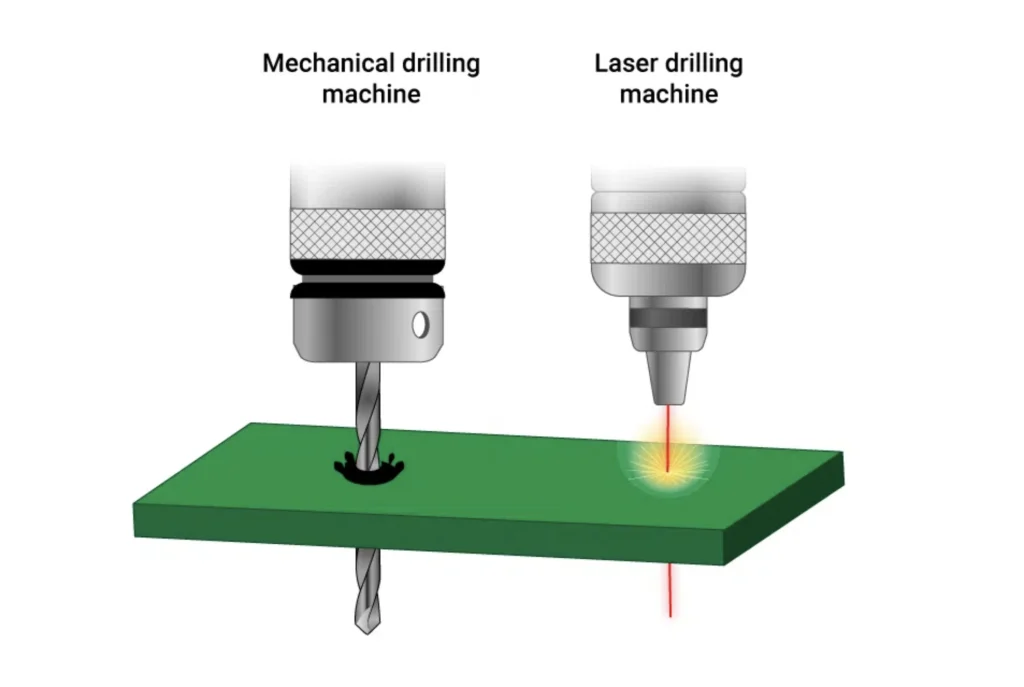
Physical attacks on ATMs, such as drilling into the machine or attempting to access the PCB, are a significant threat. Anti-tampering PCB measures are designed to detect and respond to such intrusions, protecting the hardware and the data it processes.
One effective method is the use of tamper-evident coatings or meshes on the PCB. These are thin layers or grids of conductive material that cover critical components. If an attacker tries to drill or cut through the PCB, the mesh is disrupted, triggering an alert or shutting down the system. Some designs even erase sensitive data stored in memory if tampering is detected, ensuring that no information is compromised.
Another approach involves placing critical components in hard-to-access areas of the PCB layout. For example, sensitive chips can be sandwiched between layers of the board, making it nearly impossible to probe or replace them without damaging the entire circuit. Additionally, using microvias (tiny vias with diameters as small as 0.1 mm) in the PCB design can make reverse-engineering more difficult due to their small size and complexity.
These anti-tampering measures add a vital layer of security, ensuring that even if an attacker gains physical access to an ATM, they cannot easily extract data or manipulate the system.
Cryptographic Module PCB Integration: Building Trust in Hardware
Cryptographic module PCB integration takes hardware security to the next level by embedding dedicated cryptographic hardware directly onto the board. These modules handle tasks like key generation, encryption, decryption, and digital signatures, ensuring that sensitive operations are performed in a secure environment.
A typical cryptographic module might comply with standards like FIPS 140-2 or 140-3, which define security requirements for cryptographic hardware. These modules often include features like secure key storage, random number generation, and resistance to side-channel attacks (e.g., power analysis or electromagnetic leakage). For example, a module might use differential power analysis countermeasures to prevent attackers from deducing encryption keys by monitoring power consumption fluctuations, which can vary by as little as 0.01 volts during processing.
Integrating these modules into the PCB requires careful design to minimize signal interference and ensure reliable performance. Engineers must pay attention to impedance matching, often targeting values around 50 ohms for high-speed data lines, to prevent data corruption or delays in cryptographic operations. Proper grounding and shielding are also essential to protect against electromagnetic interference, which could otherwise expose sensitive data.
Financial Data Protection PCB: A Holistic Approach
Financial data protection at the PCB level requires a combination of the techniques discussed above—hardware encryption, secure boot, anti-tampering measures, and cryptographic modules. Together, these create a multi-layered defense that safeguards ATM transactions from both digital and physical threats.
One key aspect of financial data protection PCB design is ensuring compliance with industry standards like PCI DSS (Payment Card Industry Data Security Standard). This standard mandates specific security controls for devices handling cardholder data, including encryption and secure key management. PCBs designed for ATMs must meet these requirements to avoid penalties and ensure customer trust.
Another consideration is power efficiency. Security features like encryption and secure boot can consume significant power, so PCBs must be optimized to balance security and energy use. For example, low-power encryption chips might operate at voltages as low as 1.8V, reducing overall power draw while maintaining high security levels.
Finally, regular updates to firmware and security protocols are crucial. While hardware security is robust, evolving threats mean that PCBs must support secure over-the-air updates to patch vulnerabilities. This requires additional design considerations, such as reserved memory space on the PCB for update storage and secure communication channels for data transfer.
Challenges in Designing Secure PCBs for ATMs
Designing PCBs with advanced security features for ATMs is not without challenges. One major issue is cost. High-end cryptographic modules, tamper-resistant coatings, and secure boot hardware can significantly increase production expenses. Engineers must balance security needs with budget constraints, often prioritizing the most critical features for protection.
Another challenge is complexity. Adding multiple security layers to a PCB can complicate the design process, increasing the risk of errors or performance issues. For instance, improper routing of high-speed signals for encryption modules can lead to signal integrity problems, with impedance mismatches causing data errors or delays. Careful simulation and testing, often using tools to analyze signal rise times (e.g., targeting under 1 ns for critical paths), are essential to avoid these pitfalls.
Lastly, staying ahead of evolving threats requires constant innovation. Attackers are continually developing new methods to bypass security, from advanced side-channel attacks to sophisticated physical tampering. PCB designers must stay informed about the latest security trends and adapt their designs accordingly.
Best Practices for PCB Designers in ATM Security
For engineers working on ATM PCB designs, following best practices can make a significant difference in security outcomes. First, always prioritize hardware-based security over software solutions where possible. Hardware encryption and secure boot mechanisms are harder to compromise than software patches.
Second, use layered security approaches. Combine anti-tampering measures with cryptographic modules and secure boot designs to create multiple barriers against attacks. Each layer should function independently, so a breach in one area doesn’t compromise the entire system.
Third, conduct thorough testing at every stage of development. Simulate physical and digital attacks to identify weaknesses in the PCB design. For example, test tamper-evident meshes by attempting controlled breaches and measure response times, ideally aiming for detection within 100 milliseconds of an intrusion.
Finally, collaborate with security experts during the design phase. Their insights can help identify potential vulnerabilities early, saving time and resources in the long run. Partnering with a trusted PCB manufacturing service can also ensure that designs are implemented with precision and high-quality materials.
Conclusion: Building a Safer Future for ATM Transactions
Securing ATM transactions starts at the hardware level, with PCBs playing a pivotal role in protecting financial data. Through ATM PCB hardware encryption, secure boot PCB design, anti-tampering PCB measures, cryptographic module PCB integration, and a focus on financial data protection, engineers can create systems that withstand both digital and physical threats. While challenges like cost and complexity exist, the benefits of robust security far outweigh the difficulties. By following best practices and staying ahead of evolving threats, we can build ATMs that keep customer data safe and maintain trust in financial systems.
At ALLPCB, we’re committed to supporting engineers in designing secure, high-performance PCBs for critical applications like ATMs. Our expertise and manufacturing capabilities ensure that your designs are brought to life with the highest standards of quality and precision, helping you safeguard sensitive data in every transaction.
 ALLPCB


