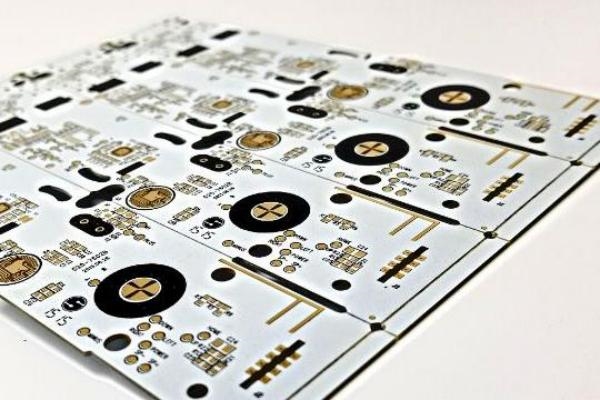
In the world of printed wiring boards (PWBs), "black pad" is a term that raises red flags for engineers and manufacturers alike. But why are black pads bad? Simply put, black pads are defects that occur during the surface finishing process of a PWB, particularly with Electroless Nickel Immersion Gold (ENIG) finishes. These defects can lead to poor solderability, weak connections, and even complete board failure, costing time and money in repairs or replacements. In this blog, we’ll dive deep into the effects of black pads, how they contribute to PWB defects, and the design considerations you need to keep in mind to avoid them. Whether you're an engineer or a manufacturer, understanding this issue is critical to ensuring reliable and high-quality boards.
What Is a Black Pad Defect?
A black pad defect refers to the corrosion or degradation of the nickel layer in an ENIG surface finish on a PWB. ENIG is a popular finish because it provides excellent solderability and corrosion resistance. It consists of a layer of nickel deposited on the copper pads of the board, topped with a thin layer of gold to protect the nickel from oxidation. However, during the manufacturing process, if the nickel layer is improperly deposited or exposed to certain conditions, it can corrode, forming a black or dark gray layer—hence the term "black pad."
This defect often goes unnoticed during initial inspections because it’s hidden beneath the gold layer. It only becomes apparent during soldering, when the connection fails to form properly, or after the board is in use, when connections weaken or break entirely. Black pad effects can be catastrophic, especially in high-reliability applications like aerospace, medical devices, or automotive systems.
The Effects of Black Pads on PWB Performance
Black pads are not just a cosmetic issue; they have serious consequences for the performance and reliability of a printed wiring board. Let’s break down the key black pad effects and why they are so problematic:
1. Poor Solderability
One of the primary black pad effects is poor solderability. The corroded nickel layer prevents the solder from properly bonding to the pad. Instead of forming a strong, reliable joint, the solder may form a weak or incomplete connection. This can lead to "open circuits," where there is no electrical connection at all, or intermittent connections that fail under stress or over time.
2. Weak Mechanical Strength
Even if a solder joint forms, the presence of a black pad can weaken the mechanical strength of the connection. The corroded nickel layer often has cracks or uneven surfaces, which create stress points in the joint. Over time, thermal cycling, vibration, or mechanical stress can cause the joint to crack or break, leading to board failure. Studies have shown that joints affected by black pads can have up to 50% less mechanical strength compared to unaffected joints.
3. Increased Risk of Failure in High-Reliability Applications
In applications where reliability is critical, such as in medical equipment or automotive electronics, black pad defects can have dire consequences. A single failed connection can cause an entire system to malfunction, potentially leading to safety hazards. For instance, a failed solder joint in a car's braking system control unit could result in catastrophic failure. The risk is simply too high to ignore black pad effects in these scenarios.
4. Costly Repairs and Rework
Black pad defects often aren’t detected until after the board is assembled or even deployed in the field. At that point, identifying and repairing the issue can be incredibly costly. Reworking a board with black pad defects may involve desoldering components, cleaning the pads, and reapplying a new finish—a process that is time-consuming and expensive. In some cases, the board may be irreparable, requiring a full replacement.
How Black Pads Contribute to PWB Defects
Black pads are a significant contributor to PWB defects because they undermine the integrity of the board at a fundamental level. Here are some of the ways they lead to broader issues:
1. Compromised Electrical Performance
The primary function of a PWB is to provide reliable electrical connections between components. When black pads prevent proper soldering, they create high-resistance paths or complete disconnections. This can lead to signal integrity issues, where electrical signals are distorted or lost. For high-speed circuits, this is especially problematic, as even small increases in resistance can degrade performance. For example, a black pad defect might increase contact resistance from a typical 1-2 milliohms to over 10 milliohms, significantly impacting signal quality.
2. Thermal Stress Failures
During operation, PWBs are exposed to temperature fluctuations that cause materials to expand and contract. A solder joint weakened by a black pad is less able to withstand these thermal stresses. Over time, this can lead to cracks in the joint or delamination of the pad from the board, resulting in a complete failure. Thermal cycling tests have shown that boards with black pad defects fail after as few as 500 cycles, compared to over 2000 cycles for defect-free boards.
3. Corrosion Propagation
Black pads don’t just stay confined to one area; the corrosion can spread to adjacent pads or layers if not addressed. This is especially true in humid or harsh environments, where moisture can accelerate the corrosion process. Once corrosion spreads, it can cause multiple PWB defects, turning a small issue into a widespread problem that affects the entire board.
Design Considerations to Avoid Black Pad Defects
Preventing black pad defects starts with careful design and manufacturing practices. By addressing potential issues early in the process, you can minimize the risk of black pad effects and other PWB defects. Here are some key design considerations:
1. Optimize ENIG Process Parameters
The root cause of black pads often lies in the ENIG plating process. During nickel deposition, factors like bath chemistry, temperature, and immersion time must be carefully controlled. If the nickel bath contains too many impurities or if the pH is not within the optimal range (typically 4.5 to 5.5), it can lead to a porous or uneven nickel layer that is prone to corrosion. Work closely with your manufacturing partner to ensure strict process controls are in place.
2. Use High-Quality Materials
The quality of the materials used in the ENIG finish plays a big role in preventing black pads. Low-quality nickel or gold solutions can introduce contaminants that increase the likelihood of corrosion. Specify high-purity materials and verify that your supplier adheres to industry standards, such as IPC-4552, which outlines performance specifications for ENIG finishes.
3. Design for Proper Pad Geometry
The geometry of the pads on your PWB can also influence the risk of black pad defects. Smaller pads or pads with irregular shapes may not receive uniform nickel and gold deposition, increasing the chance of defects. Ensure that pad sizes and shapes are designed to allow for even plating. For example, maintaining a minimum pad diameter of 0.25 mm for surface-mount components can help achieve consistent results.
4. Implement Rigorous Testing and Inspection
Early detection is key to avoiding the consequences of black pad defects. Incorporate rigorous testing and inspection into your quality control process. Techniques like X-ray fluorescence (XRF) can measure the thickness and uniformity of the nickel and gold layers, while cross-sectional analysis can reveal hidden corrosion. Testing should be done both during manufacturing and after assembly to catch issues before they become costly failures.
5. Consider Alternative Surface Finishes
If black pad defects are a recurring issue or if your application is particularly sensitive to reliability concerns, consider alternative surface finishes. Options like Immersion Silver or Organic Solderability Preservative (OSP) may be less prone to corrosion-related defects, though they come with their own trade-offs in terms of cost and performance. Evaluate the needs of your specific project to determine the best finish.
Steps to Mitigate Black Pad Effects During Manufacturing
Beyond design considerations, there are practical steps you can take during manufacturing to reduce the risk of black pad effects:
- Monitor Bath Chemistry: Regularly test and adjust the chemical composition of the nickel and gold plating baths to prevent contamination or imbalance.
- Control Immersion Time: Avoid over-immersion during the gold plating process, as excessive time can lead to nickel corrosion. Typical immersion times should be kept between 5-10 minutes, depending on the specific process.
- Maintain Cleanliness: Ensure that the PWB surfaces are free of contaminants before plating. Even small amounts of organic residue or oxidation on the copper can interfere with nickel deposition.
- Train Personnel: Equip manufacturing staff with the knowledge and skills to recognize and address potential issues during the ENIG process.
Conclusion: Protect Your PWBs from Black Pad Defects
Black pads are bad news for any printed wiring board. Their effects—ranging from poor solderability to complete board failure—can compromise the performance and reliability of your electronic products. By understanding the causes and consequences of black pad defects, and by implementing smart design considerations and manufacturing practices, you can significantly reduce the risk of these issues. Prioritizing quality control, optimizing the ENIG process, and staying vigilant during production are all essential steps to ensuring your PWBs are defect-free and built to last.
At ALLPCB, we’re committed to helping you achieve the highest standards of quality in your PWB projects. By focusing on precision and reliability at every stage, we aim to deliver boards that meet your exact specifications without the worry of defects like black pads. Trust us to be your partner in creating durable, high-performance electronics.
 ALLPCB


