 ALLPCB


In the world of printed circuit board (PCB) design and manufacturing, achieving reliable interconnects is crucial for high-performance electronics. One key factor in this process is blind via depth control. But what exactly does this mean, and how can manufacturers ensure precision in blind via drill depth accuracy? Simply put, blind via depth control involves precisely drilling holes that connect specific layers of a PCB without penetrating through the entire board, ensuring electrical connectivity and structural integrity. In this blog, we’ll dive deep into the methods, tolerances, and technologies behind controlled depth drilling for blind vias, providing actionable insights for engineers and designers looking to optimize their PCB designs.
What Are Blind Vias and Why Do They Matter?
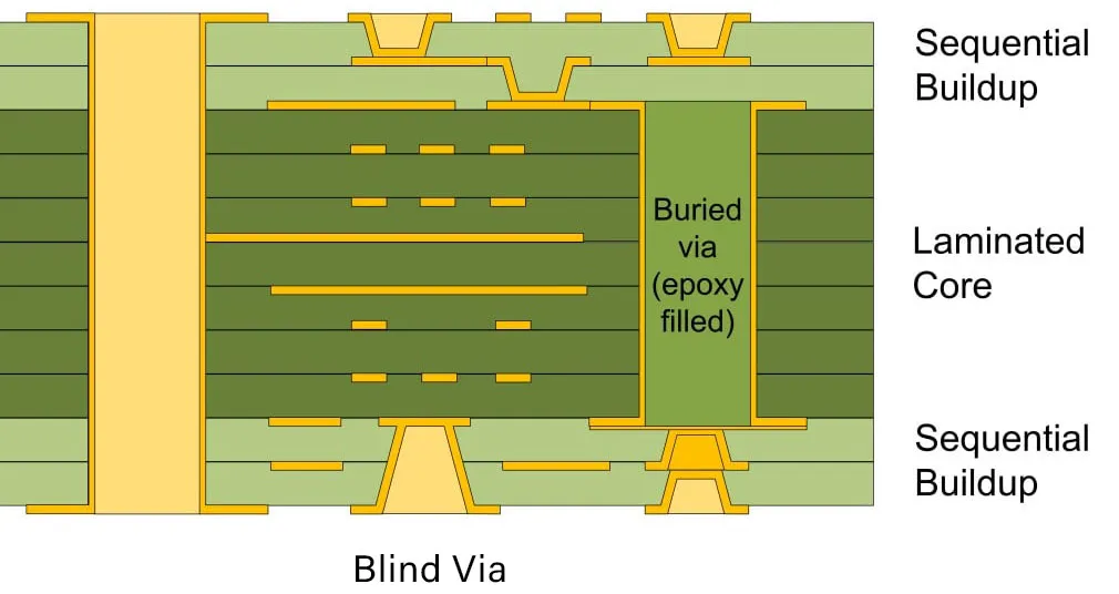
Blind vias are vertical interconnects in a PCB that connect an outer layer to one or more inner layers without passing through the entire board. Unlike through-hole vias, which span the full thickness of the PCB, blind vias are only visible on one side, making them ideal for high-density interconnect (HDI) designs where space is limited. They play a vital role in modern electronics, enabling compact designs for devices like smartphones, wearables, and advanced medical equipment.
The importance of blind via depth control methods cannot be overstated. If the depth of a blind via is inaccurate, it can lead to poor electrical connections, signal integrity issues, or even structural damage to the PCB. For instance, drilling too deep might damage underlying layers, while insufficient depth can result in weak or non-existent connections. This is why precision in blind via depth tolerance is a top priority for manufacturers aiming to deliver reliable and high-performing boards.
Challenges in Blind Via Depth Control
Drilling blind vias with precision is no easy task. Several challenges can affect blind via drill depth accuracy, including:
- Material Variations: PCBs are made of multiple layers of materials like copper, resin, and fiberglass, each with different hardness levels. These variations can cause drill bits to deviate or wear unevenly, impacting depth control.
- Aspect Ratio Limitations: Blind vias often have a high aspect ratio (depth-to-diameter ratio), typically around 5:1 or less. Exceeding this ratio can lead to drilling inaccuracies or incomplete plating, affecting connectivity.
- Equipment Precision: The accuracy of drilling equipment, whether mechanical or laser-based, directly influences depth control. Older or poorly calibrated machines may struggle to maintain tight tolerances.
- Layer Alignment: Misalignment between layers during the stacking process can result in blind vias missing their target inner layer, leading to connectivity failures.
Addressing these challenges requires advanced techniques and strict quality control measures to ensure that every blind via meets design specifications.
Methods for Blind Via Depth Control
Achieving precise controlled depth drilling for blind vias involves a combination of advanced technologies and meticulous processes. Below are some of the most effective blind via depth control methods used in the industry today:
1. Mechanical Controlled Depth Drilling
Mechanical drilling is a traditional method for creating blind vias, especially in standard PCB designs. In controlled depth drilling, the drill bit is programmed to penetrate only to a specific depth, stopping before it reaches the next layer or the opposite side of the board. Modern CNC (Computer Numerical Control) drilling machines can achieve depth tolerances as tight as ±0.05 mm, depending on the equipment and material stack-up.
However, mechanical drilling has limitations, especially for very small vias or high-density designs. Drill bit wear and material inconsistencies can affect precision, making it less ideal for microvias (vias with diameters below 0.15 mm).
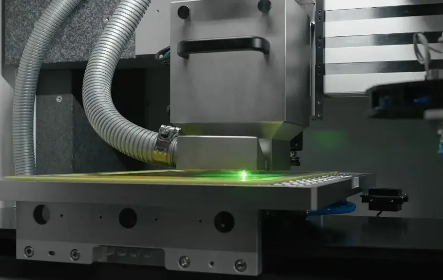
2. Laser Drilling for Microvias
For HDI boards requiring smaller vias, laser drilling is the preferred method. Lasers can create vias with diameters as small as 0.1 mm and achieve exceptional blind via depth tolerance of ±0.02 mm or better. This method uses focused beams to ablate material layer by layer, offering greater control over depth and minimizing damage to surrounding areas.
Laser drilling is particularly effective for blind vias in thin dielectric layers, often found in advanced consumer electronics. However, it requires specialized equipment and can be more costly than mechanical drilling.

3. Back Drilling Technique
Back drilling is a technique often used in high-speed PCB designs to remove excess via stubs that can cause signal reflection and impedance mismatch. While not exclusively for blind vias, it can be adapted to control depth in specific scenarios. Advanced back drilling methods can achieve depth control within ±0.1 mm, ensuring that only the necessary portion of the via remains conductive.
This method is particularly useful in designs where signal integrity is critical, such as in telecommunications or data centers, where signal speeds can exceed 10 Gbps.
4. Depth Sensing and Feedback Systems
Modern drilling machines often incorporate depth-sensing technologies, such as contact sensors or laser-based measurement systems, to monitor and adjust drilling depth in real-time. These systems can detect when the drill reaches the target layer by sensing changes in material properties or electrical conductivity. This feedback loop enhances blind via drill depth accuracy, reducing the risk of over-drilling or under-drilling.
5. Process Validation and Testing
Beyond drilling techniques, manufacturers use various testing methods to validate blind via depth tolerance. X-ray inspection and cross-sectional analysis are common ways to verify that vias are drilled to the correct depth and properly plated for conductivity. These quality control steps are essential for catching errors before the PCB moves to assembly.
Factors Influencing Blind Via Depth Tolerance
Maintaining tight blind via depth tolerance is critical for ensuring reliable interconnects. Several factors influence the achievable tolerance levels:
- Drilling Equipment: High-end CNC and laser drilling machines can maintain tolerances of ±0.02 to ±0.05 mm, while older equipment may only achieve ±0.1 mm or worse.
- Material Stack-Up: The thickness and composition of PCB layers affect how easily depth can be controlled. For example, drilling through a 0.2 mm dielectric layer requires more precision than a 1.6 mm standard board.
- Via Size: Smaller vias, such as microvias with diameters of 0.15 mm or less, demand tighter tolerances to avoid issues like incomplete plating or misalignment.
- Design Rules: Adhering to manufacturer-specific design guidelines, such as maintaining a minimum annular ring of 0.1 mm around vias, helps ensure accurate drilling and plating.
By optimizing these factors, manufacturers can achieve the precision needed for even the most demanding PCB designs.
Best Practices for Designing Blind Vias
For engineers and designers, incorporating blind vias into a PCB layout requires careful planning to ensure manufacturability and reliability. Here are some best practices to follow:
- Define Clear Depth Specifications: Work closely with your manufacturing partner to specify the exact depth for each blind via, accounting for layer thickness and tolerances.
- Limit Aspect Ratios: Keep the depth-to-diameter ratio of blind vias below 5:1 to avoid drilling and plating challenges.
- Use Proper Pad Sizes: Ensure that pads around blind vias have sufficient annular rings (at least 0.1 mm) to accommodate potential misalignment during drilling.
- Specify Fill Type: Depending on the application, decide whether blind vias should be filled with epoxy or copper plugs to enhance thermal or electrical performance.
- Validate with Simulations: Use PCB design software to simulate signal integrity and impedance, especially for high-speed designs where blind vias impact performance.
Following these guidelines can significantly reduce the risk of errors during manufacturing and ensure that blind vias perform as intended.
Applications of Blind Vias with Controlled Depth
Blind vias are widely used in various industries where space constraints and performance requirements demand advanced PCB designs. Some common applications include:
- Consumer Electronics: Smartphones and tablets rely on HDI boards with blind vias to pack more functionality into smaller spaces.
- Automotive Systems: Advanced driver-assistance systems (ADAS) use blind vias for compact, high-reliability interconnects in harsh environments.
- Medical Devices: Wearable health monitors and diagnostic equipment benefit from the space-saving and performance advantages of blind vias.
- Telecommunications: High-speed data transfer equipment requires blind vias to minimize signal loss and maintain impedance control at speeds exceeding 25 Gbps.
In each of these applications, precise controlled depth drilling for blind vias ensures that the interconnects are reliable and efficient, meeting the strict demands of modern technology.
The Future of Blind Via Technology
As electronics continue to shrink in size and increase in complexity, the demand for precise blind via depth control will only grow. Emerging trends in PCB manufacturing, such as the adoption of advanced laser drilling systems and AI-driven quality control, promise to further improve blind via drill depth accuracy. Additionally, new materials with better thermal and electrical properties are being developed to support even tighter tolerances and higher performance.
Manufacturers are also exploring automation and real-time monitoring to enhance depth control during production. These advancements will make it easier to produce complex HDI boards with blind vias, opening up new possibilities for innovation in electronics design.
Conclusion
Blind vias are a cornerstone of modern PCB design, enabling compact, high-performance electronics through reliable interconnects. However, their effectiveness depends heavily on precise blind via depth control. By leveraging advanced blind via depth control methods like laser drilling, controlled depth mechanical drilling, and real-time feedback systems, manufacturers can achieve the tight blind via depth tolerance needed for today’s demanding applications.
For engineers and designers, understanding the challenges and best practices associated with controlled depth drilling for blind vias is essential for creating successful PCB layouts. By prioritizing precision and collaboration with manufacturing partners, you can ensure that your designs meet performance and reliability standards, no matter the complexity.
At ALLPCB, we are committed to providing cutting-edge solutions for blind via manufacturing, helping you bring your innovative designs to life with unmatched accuracy and quality. Whether you’re working on consumer electronics, automotive systems, or telecommunications equipment, our expertise in blind via technology is here to support your success.


