 ALLPCB


In the world of PCB design, getting the right trace width and impedance is like finding the perfect harmony in a song. If you’ve ever searched for terms like "pcb trace impedance calculator," "controlled impedance trace width," "impedance matching pcb," or "signal integrity trace width," you’re likely looking for ways to ensure your circuit board performs flawlessly. The short answer? Trace width and impedance must work together to maintain signal integrity, prevent signal loss, and avoid interference in high-speed designs.
In this detailed guide, we’ll break down the relationship between trace width and impedance, why it matters, and how you can calculate and control these factors for optimal PCB performance. Whether you’re a beginner or a seasoned engineer, this blog will provide actionable insights to elevate your designs. Let’s dive in!
What Are Trace Width and Impedance in PCB Design?
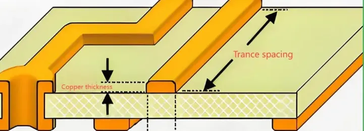
Before we explore their relationship, let’s define the basics. Trace width refers to the physical width of the copper paths on a printed circuit board (PCB) that carry electrical signals or power. Impedance, on the other hand, is a measure of opposition to the flow of alternating current (AC) in a circuit, influenced by resistance, capacitance, and inductance. In PCB terms, it’s often called characteristic impedance, which is critical for high-speed signals.
Why do these two factors matter together? In high-speed designs, like those for USB, HDMI, or DDR memory, mismatched impedance can lead to signal reflections, crosstalk, and data loss. Trace width plays a huge role in determining impedance, alongside other factors like dielectric material, trace thickness, and PCB layer stack-up. Getting this balance right ensures your signals travel smoothly without distortion.
Why Impedance Matching Matters for Signal Integrity
Impedance matching in PCB design is the process of ensuring that the impedance of a trace matches the source and load impedance of the connected components. When there’s a mismatch, part of the signal reflects back, causing noise and degrading signal integrity. This is especially problematic in high-speed circuits where even tiny reflections can corrupt data.
For example, in a 50-ohm system (common for RF and high-speed digital signals), if your trace impedance deviates to 60 ohms due to incorrect trace width, you could see up to 9% of the signal reflected back. This might not sound like much, but at gigabit speeds, it can mean the difference between a working design and a failed one.
Trace width directly affects impedance. A wider trace typically has lower impedance because it reduces resistance and increases capacitance with the ground plane. Conversely, a narrower trace increases impedance. Balancing this relationship is key to achieving proper impedance matching for your PCB.
How Trace Width Impacts Controlled Impedance
Controlled impedance is a design technique where trace impedance is deliberately set to a specific value (like 50 ohms or 100 ohms for differential pairs) to ensure consistent signal transmission. Trace width is one of the primary factors designers adjust to achieve this.
Let’s break it down with numbers. For a standard FR-4 PCB material with a dielectric constant of 4.5, a trace height of 1.6 mm above the ground plane, and a copper thickness of 1 oz (35 micrometers), you might need a trace width of about 0.3 mm to achieve a 50-ohm impedance for a single-ended microstrip line. If you increase the width to 0.5 mm, the impedance could drop to around 40 ohms, causing a mismatch.
Other factors, like the spacing between traces in differential pairs or the PCB stack-up, also play a role. But trace width remains a critical lever for fine-tuning impedance. This is why understanding "controlled impedance trace width" is so vital for high-speed designs.
Signal Integrity and Trace Width: A Balancing Act
Signal integrity refers to the quality of an electrical signal as it travels through a PCB. Poor signal integrity can result in data errors, electromagnetic interference (EMI), and system failures. Trace width impacts signal integrity in two major ways: current-carrying capacity and impedance control.
For power traces, wider traces are better because they can handle more current without overheating. A common guideline is that a 10-mil (0.254 mm) wide trace on 1 oz copper can carry about 0.5 amps safely, assuming a temperature rise of 10°C. But for high-speed signal traces, wider isn’t always better. As mentioned earlier, wider traces lower impedance, which might not match the system’s requirements.
Finding the right "signal integrity trace width" means balancing these needs. Too narrow, and you risk signal loss due to high resistance or overheating. Too wide, and you disrupt impedance matching, leading to reflections. This is where design tools and calculations come into play.
Using a PCB Trace Impedance Calculator for Precision
Calculating trace width and impedance by hand can be complex due to the many variables involved—dielectric constant, trace height, copper thickness, and more. This is where a "pcb trace impedance calculator" becomes invaluable. These tools use mathematical models, like the microstrip or stripline equations, to estimate the required trace width for a target impedance.
For instance, let’s say you’re designing a 100-ohm differential pair for a high-speed USB interface. You input parameters like dielectric constant (4.2 for FR-4), trace spacing (0.2 mm), and PCB thickness (1.6 mm) into the calculator. The tool might suggest a trace width of 0.15 mm per trace to achieve the desired impedance. Without such a tool, you’d spend hours solving equations or running simulations.
Many online calculators are available for free and can handle both single-ended and differential impedance calculations. They often include options for different PCB configurations, such as microstrip (traces on the surface) or stripline (traces between layers). Using these tools ensures precision and saves time in the design process.
Steps to Achieve Impedance Matching in Your PCB Design
Now that we understand the theory, let’s walk through practical steps to achieve "impedance matching pcb" design using trace width and other factors. Follow this process to ensure your board performs as intended:
- Define Your Impedance Requirements: Determine the target impedance for your traces based on the components and standards you’re using. For example, USB 2.0 often requires 90 ohms for differential pairs, while Ethernet might need 100 ohms.
- Choose the Right Materials: Select a PCB substrate with a consistent dielectric constant. FR-4 is common, with a dielectric constant of about 4.2–4.5, but high-speed designs might need materials like Rogers with lower loss.
- Set Up Your Stack-Up: Design your PCB layers to minimize variations in trace height and ground plane spacing, as these affect impedance.
- Calculate Trace Width: Use a PCB trace impedance calculator to find the optimal trace width for your target impedance. Adjust for single-ended or differential traces as needed.
- Simulate and Test: Use simulation software to verify impedance before manufacturing. After production, test with a time-domain reflectometer (TDR) to confirm the impedance matches your design.
By following these steps, you can minimize signal reflections and ensure reliable performance in your PCB designs.
Common Challenges in Trace Width and Impedance Design
Even with the best tools, challenges can arise when designing for controlled impedance. Here are some common issues and how to address them:
- Manufacturing Tolerances: PCB fabrication processes can introduce variations in trace width (typically ±10%) and dielectric thickness, affecting impedance. Work closely with your manufacturer to understand their tolerances and design with some margin.
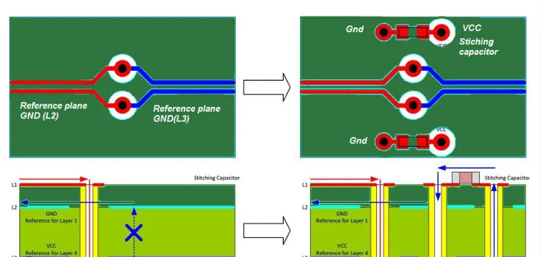
- Trace Routing Constraints: Limited board space might force you to route traces closer together or over split ground planes, disrupting impedance. Use wider spacing where possible and avoid routing over gaps in ground planes.
- High-Frequency Effects: At very high frequencies (above 1 GHz), skin effect and dielectric losses become significant, altering effective impedance. Consider using low-loss materials and wider traces for such designs.
Being aware of these pitfalls can help you design more robust PCBs that maintain signal integrity under real-world conditions.
Tips for Optimizing Trace Width and Impedance
To wrap up, here are some practical tips for mastering trace width and impedance in your PCB designs:
- Start with Standards: Follow industry standards like IPC-2141 for controlled impedance design to ensure consistency and reliability.
- Use Ground Planes: Place continuous ground planes beneath signal traces to provide a stable reference for impedance and reduce EMI.
- Keep Traces Short: Minimize trace length for high-speed signals to reduce the chance of impedance mismatch and signal delay.
- Iterate with Tools: Use simulation tools alongside calculators to test different trace widths and stack-ups before finalizing your design.
- Collaborate with Manufacturers: Share your impedance requirements with your PCB fabricator early in the process to ensure they can meet your specifications.
Conclusion: Building Better PCBs with Trace Width and Impedance Harmony
Trace width and impedance are two sides of the same coin in PCB design. When they’re aligned, you get a board that delivers clean signals, minimal interference, and reliable performance—truly a match made in PCB heaven. By leveraging tools like a "pcb trace impedance calculator," focusing on "controlled impedance trace width," mastering "impedance matching pcb" techniques, and optimizing "signal integrity trace width," you can take your designs to the next level.
Whether you’re working on a simple prototype or a complex high-speed system, understanding and controlling these factors is essential. With the steps and tips provided in this guide, you’re well-equipped to tackle impedance challenges and build PCBs that perform flawlessly. Keep experimenting, calculating, and refining your designs, and you’ll see the difference in every project.


