 ALLPCB


If you're a PCB designer looking to master rigid-flex PCB design, especially the critical flex-to-rigid transition zones, you're in the right place. This guide offers a detailed rigid-flex PCB design tutorial, explores flex PCB transition zone best practices, and provides actionable tips for designing reliable flex-to-rigid interfaces. Whether you're new to rigid-flex designs or refining your skills, you'll find practical advice to ensure your boards are durable, efficient, and ready for manufacturing.
In the sections below, we'll dive deep into the fundamentals of rigid-flex technology, the importance of transition zones, and step-by-step strategies to optimize your designs. Let's get started on building better, more reliable PCBs.
What Are Rigid-Flex PCBs and Why Do They Matter?
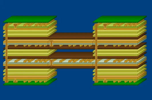
Rigid-flex PCBs combine the benefits of rigid and flexible circuit boards into a single design. The rigid sections provide structural support for components, while the flexible sections allow the board to bend or fold, enabling compact and dynamic layouts. This hybrid technology is widely used in industries like aerospace, medical devices, and consumer electronics, where space constraints and reliability are critical.
The key challenge in rigid-flex design lies in the transition zones—the areas where the flexible material meets the rigid substrate. Poorly designed transitions can lead to mechanical stress, signal integrity issues, or even board failure. Mastering these interfaces is essential for creating robust designs that withstand repeated bending and environmental stress.
Understanding the Flex-to-Rigid Transition Zone
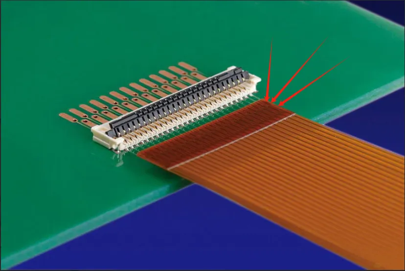
The flex-to-rigid transition zone is the boundary where the flexible polyimide material connects to the rigid FR4 or other substrate. This area is prone to mechanical strain because of the differing properties of the materials. During bending, the flexible section moves while the rigid section remains static, creating stress points that can cause cracks, delamination, or trace damage.
To design reliable flex-to-rigid interfaces, you must account for material properties, layer stack-up, and the intended application. For instance, a wearable device might require hundreds of thousands of bend cycles, while an automotive application might prioritize thermal stability over flexibility. Understanding the specific demands of your project is the first step in optimizing the transition zone.
Key Challenges in Transition Zones
- Mechanical Stress: Repeated bending can fatigue the materials, leading to cracks or breaks.
- Signal Integrity: Abrupt changes in material can disrupt impedance, causing signal loss or noise, especially in high-speed designs operating at frequencies above 1 GHz.
- Manufacturing Complexity: Misalignment or improper bonding in the transition zone can result in defects during fabrication.
Addressing these challenges requires careful planning and adherence to best practices, which we'll explore next.
Flex PCB Transition Zone Best Practices
Designing a reliable transition zone is critical for the longevity and performance of your rigid-flex PCB. Below are proven strategies to minimize stress and ensure durability.
1. Use Gradual Transitions
Avoid sharp or abrupt changes between the rigid and flexible sections. Instead, design a gradual taper or curve in the transition area to distribute stress more evenly. For example, extending the rigid material slightly into the flex area as a "stiffener" can reduce strain. Many designers aim for a transition length of at least 0.5 mm to 1 mm to achieve this effect.
2. Optimize Layer Stack-Up
The layer stack-up defines how the rigid and flexible materials are bonded. A common approach is to use a no-flow prepreg (a type of bonding material) in the rigid areas to prevent adhesive from flowing into the flex section during lamination. Additionally, ensure that copper traces in the transition zone are kept thin—typically 0.5 oz to 1 oz—to reduce stiffness and prevent cracking.
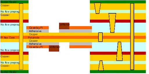
3. Reinforce with Stiffeners
Stiffeners, often made of polyimide or FR4, can be added to the flex section near the transition zone to provide extra support. This is especially useful in applications with frequent bending. However, avoid placing stiffeners directly over high-speed signal lines, as they can interfere with impedance control. For instance, in a design with signals running at 2.5 GHz, a stainless steel stiffener could introduce unwanted noise if placed too close to critical traces.
4. Manage Bend Radius
The bend radius—the curvature of the flex section—should be at least 10 times the thickness of the flex material to prevent damage. For a flex layer thickness of 0.1 mm, maintain a minimum bend radius of 1 mm. Tighter bends increase stress in the transition zone, leading to potential failure over time.
Designing Reliable Flex-to-Rigid Interfaces: Step-by-Step Tutorial
Now that we've covered the best practices, let's walk through a rigid-flex PCB design tutorial focused on creating reliable flex-to-rigid interfaces. These steps are tailored for designers working on compact, high-performance boards.
Step 1: Define Design Requirements
Start by identifying the mechanical and electrical needs of your project. How many bend cycles will the board endure? What are the impedance requirements for high-speed signals? For example, a medical device might need to handle 100,000 bend cycles, while a telecommunications board might require controlled impedance of 50 ohms for signal integrity.
Step 2: Select Materials Carefully
Choose materials that match your application. Polyimide is the standard for flex layers due to its durability and thermal resistance, with a typical thickness of 25 to 50 micrometers. For rigid sections, FR4 with a thickness of 0.8 mm to 1.6 mm provides adequate support. Ensure that the adhesive used in the transition zone is compatible with both materials to avoid delamination.
Step 3: Plan Trace Routing in Transition Zones
Route traces perpendicular to the bend line in the transition zone to minimize stress. Avoid placing vias or pads directly in this area, as they can act as stress concentrators. If high-speed signals are involved, maintain a consistent ground plane to avoid impedance mismatches. For instance, a signal running at 5 GHz could experience a 10% signal loss if the ground plane is interrupted in the transition zone.
Step 4: Test and Simulate
Use simulation tools to model mechanical stress and signal integrity in the transition zone. Software like finite element analysis (FEA) can predict stress points during bending, while signal integrity simulators can identify impedance issues. Adjust your design based on these results to ensure reliability before moving to fabrication.
Step 5: Collaborate with Manufacturers
Work closely with your PCB manufacturer during the design phase. Share detailed stack-up drawings and specify tolerances for the transition zone. Many manufacturing issues, such as misalignment, can be avoided by aligning your design with the fabricator's capabilities. For example, confirm that the manufacturer can achieve a bonding accuracy of ±0.1 mm in the transition area.
Common Mistakes to Avoid in Rigid-Flex Design
Even experienced designers can make errors when working with rigid-flex PCBs. Here are some pitfalls to watch out for:
- Ignoring Bend Radius: Designing a flex section with too tight a bend radius can lead to cracks. Always adhere to the 10x thickness rule.
- Overloading Transition Zones: Placing components or heavy copper in the transition area adds unnecessary stress. Keep this zone clear of non-essential elements.
- Poor Material Matching: Using incompatible adhesives or materials with mismatched thermal expansion coefficients can cause delamination over time.
Advanced Tips for High-Performance Designs
For designers working on cutting-edge applications, consider these advanced strategies to push your rigid-flex designs further:
Controlled Impedance in Transition Zones
High-speed designs often require precise impedance control. Use a dielectric material with a consistent thickness in the flex section to maintain impedance values, typically around 50 ohms for single-ended signals. Avoid abrupt changes in trace width or spacing as signals cross the transition zone, as even a 5% mismatch can degrade performance at frequencies above 3 GHz.
Thermal Management
In applications with high thermal loads, such as automotive electronics, ensure that the transition zone can handle temperature fluctuations. Use materials with low coefficients of thermal expansion (CTE) to minimize stress. For example, polyimide has a CTE of around 20 ppm/°C, which pairs well with FR4 at similar values.
Conclusion: Building Better Rigid-Flex PCBs
Mastering flex-to-rigid transitions is a game-changer for PCB designers. By following this rigid-flex PCB design tutorial, applying flex PCB transition zone best practices, and focusing on designing reliable flex-to-rigid interfaces, you can create boards that are both innovative and dependable. From gradual transitions and proper material selection to careful trace routing and manufacturer collaboration, every detail matters in ensuring the success of your design.
With the strategies and steps outlined in this guide, you're well-equipped to tackle the challenges of rigid-flex design. Keep refining your skills, stay updated on industry trends, and always prioritize the needs of your specific application. Your next project could set a new standard for performance and reliability in PCB design.


