 ALLPCB


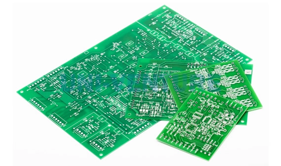
If you're looking for guidance on designing with CEM-1 for single-sided PCB layouts, you've come to the right place. CEM-1 is a popular low-cost material for single-layer printed circuit boards, often used in consumer electronics and simple designs. In this comprehensive guide, we'll cover essential CEM-1 PCB design rules, single-layer PCB layout tips, strategies for CEM-1 PCB impedance control, recommendations for the best software for CEM-1 PCB design, and effective thermal management for CEM-1. Whether you're a beginner or an experienced engineer, this post will provide actionable insights to optimize your designs.
What is CEM-1, and Why Use It for Single-Sided PCBs?
CEM-1, short for Composite Epoxy Material-1, is a laminate material made of a woven glass fabric core combined with paper and epoxy resin. It is widely used for single-layer PCBs due to its affordability and adequate mechanical strength. Compared to higher-grade materials like FR-4, CEM-1 has lower thermal resistance and dielectric properties, making it suitable for low-frequency, non-critical applications such as LED lighting, power supplies, and basic consumer gadgets.
Using CEM-1 for single-sided PCBs keeps production costs down while maintaining acceptable performance for simpler circuits. However, its limitations in thermal conductivity and electrical properties require careful design practices to ensure reliability. Let’s dive into the best practices for working with this material.
CEM-1 PCB Design Rules: Key Guidelines for Success
Designing with CEM-1 requires adherence to specific rules to compensate for its material limitations. Here are the core CEM-1 PCB design rules to follow for a successful single-sided layout:
- Trace Width and Spacing: Since CEM-1 is often used in low-cost designs, ensure trace widths are sufficient to handle current loads. A minimum trace width of 6 mils (0.15 mm) is recommended for standard applications, with spacing of at least 6 mils to avoid short circuits during manufacturing.
- Pad Sizes: Use larger pad sizes for through-hole components to improve soldering reliability on CEM-1’s less robust surface. A pad diameter of 1.5 to 2 times the hole size is a good rule of thumb.
- Avoid High-Density Designs: CEM-1 is not ideal for densely packed components due to its lower mechanical strength. Keep component spacing generous to prevent stress on the board during assembly or operation.
- Limit Operating Temperatures: CEM-1 has a lower glass transition temperature (Tg) of around 110°C compared to FR-4’s 130-140°C. Design circuits to operate below 85°C to avoid material degradation.
Following these rules ensures that your CEM-1 PCB remains durable and functional despite the material’s constraints. Always double-check manufacturer specifications for additional guidelines tailored to their processes.
Single-Layer PCB Layout Tips: Optimizing Your Design
Single-sided PCBs are inherently limited by having traces on only one side, so layout optimization is critical. Here are some practical single-layer PCB layout tips to maximize performance with CEM-1:
- Minimize Trace Lengths: Keep signal traces as short as possible to reduce noise and signal loss. For digital circuits, aim for trace lengths under 10 inches (25 cm) to maintain signal integrity at frequencies below 10 MHz.
- Use Jumpers Sparingly: Since you can’t route traces on a second layer, jumpers may be necessary. Place them strategically to avoid clutter and ensure they don’t interfere with other components.
- Group Components by Function: Arrange components in functional blocks (e.g., power, signal, output) to simplify routing and reduce cross-talk. For example, place power components near the input to minimize long power traces.
- Plan for Grounding: Even on a single-sided board, a solid ground plane is essential. If a full plane isn’t possible, create a ground grid using wide traces to provide a low-resistance path for return currents.
These tips help overcome the inherent challenges of single-layer designs, ensuring your CEM-1 PCB performs reliably in its intended application.
CEM-1 PCB Impedance Control: Challenges and Solutions
Impedance control is a critical aspect of PCB design, even for single-sided boards. However, achieving precise CEM-1 PCB impedance control can be challenging due to the material’s inconsistent dielectric constant (Dk), which typically ranges from 4.2 to 5.0, compared to FR-4’s more stable 4.3 to 4.7. Here’s how to manage impedance on CEM-1:
- Calculate Trace Widths for Impedance: Use an impedance calculator to determine the trace width needed for a target impedance, such as 50 ohms for RF applications. For example, on a 1.6 mm thick CEM-1 board with a Dk of 4.5, a 50-ohm trace may require a width of approximately 2.2 mm.
- Minimize Variations: Since CEM-1’s dielectric properties can vary across batches, avoid designs requiring tight impedance tolerances (e.g., ±5%). Stick to applications where a ±10% variation is acceptable.
- Avoid High-Frequency Signals: CEM-1 is not suited for high-frequency designs above 100 MHz due to signal loss and poor impedance stability. If higher frequencies are needed, consider alternative materials.
For most low-frequency applications on CEM-1, impedance control is manageable with careful planning. However, always test prototypes to confirm performance under real-world conditions.
Thermal Management for CEM-1: Keeping Your PCB Cool
One of the biggest drawbacks of CEM-1 is its poor thermal conductivity, which is typically around 0.3 W/m·K compared to FR-4’s 0.8 W/m·K. Effective thermal management for CEM-1 is essential to prevent overheating and ensure long-term reliability. Here are some strategies:
- Use Larger Copper Areas: Increase the copper area around heat-generating components like power resistors or ICs to act as a heat sink. For instance, a copper pour of 2 square inches (13 cm2) can reduce temperature by 5-10°C around a component dissipating 1 watt.
- Strategic Component Placement: Place heat-sensitive components away from high-power elements. Maintain at least 0.5 inches (1.27 cm) of spacing between heat sources and critical components like microcontrollers.
- Add Ventilation: If your design allows, incorporate slots or holes in the PCB near heat sources to improve airflow. Ensure these do not compromise the board’s structural integrity.
- Limit Power Dissipation: Design circuits to minimize power dissipation on the board. For example, use external heat sinks or off-board power regulators for high-current applications above 2 amps.
By applying these thermal management techniques, you can mitigate the risk of overheating and extend the lifespan of your CEM-1 PCB, even in moderately demanding environments.
Best Software for CEM-1 PCB Design: Tools to Simplify the Process
Choosing the right design software can make a significant difference when working with CEM-1 single-sided PCBs. Here are some of the best software for CEM-1 PCB design, focusing on user-friendly and cost-effective options suitable for this material:
- KiCad: A free, open-source tool that offers robust features for single-layer PCB design. It includes a built-in calculator for trace widths and impedance, which is helpful for CEM-1’s unique properties.
- Altium Designer: A professional-grade software with advanced layout and simulation tools. It’s ideal for engineers needing precise control over thermal and impedance parameters, though it comes with a higher cost.
- EAGLE: Popular among hobbyists and small businesses, this software provides an intuitive interface for single-sided layouts and supports basic thermal analysis.
These tools offer libraries and features tailored to single-layer designs, making it easier to adhere to CEM-1 design constraints. Many also provide free versions or trial periods, allowing you to test them before committing. Regardless of the software, ensure it supports exporting Gerber files for manufacturing compatibility.
Common Pitfalls to Avoid When Designing with CEM-1
Even with the best practices in mind, certain mistakes can compromise your CEM-1 PCB design. Here are some common pitfalls and how to avoid them:
- Overloading the Board: Don’t push CEM-1 beyond its limits by designing high-power or high-frequency circuits. Stick to applications with current below 5 amps and frequencies under 10 MHz.
- Ignoring Environmental Factors: CEM-1 is more prone to moisture absorption than other materials, which can affect performance. Design with protective coatings or enclosures if the board will be exposed to humidity above 70%.
- Poor Trace Routing: Avoid sharp corners in traces, as they can create stress points on CEM-1’s less durable surface. Use 45-degree angles or curves for smoother routing.
By steering clear of these issues, you can prevent costly redesigns and ensure your PCB meets performance expectations.
Manufacturing Considerations for CEM-1 Single-Sided PCBs
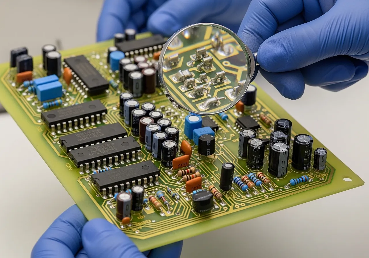
Designing a PCB is only half the battle; manufacturing plays a crucial role in the final product’s quality. When working with CEM-1, keep these manufacturing considerations in mind:
- Communicate Material Constraints: Inform your manufacturer that you’re using CEM-1 so they can adjust their processes, such as soldering temperatures, to avoid damaging the board.
- Request Prototypes: Due to CEM-1’s variability, order a small batch of prototypes to test for issues like delamination or poor solder adhesion before full production.
- Specify Surface Finish: Opt for a surface finish like HASL (Hot Air Solder Leveling) for CEM-1, as it’s cost-effective and compatible with the material’s properties.
Collaboration with your manufacturing partner ensures that your design translates smoothly from concept to finished product.
Conclusion: Mastering CEM-1 Single-Sided PCB Design
Designing with CEM-1 for single-sided PCBs offers a cost-effective solution for many applications, but it demands careful attention to detail. By following the CEM-1 PCB design rules, applying single-layer PCB layout tips, managing CEM-1 PCB impedance control, using the best software for CEM-1 PCB design, and prioritizing thermal management for CEM-1, you can create reliable and efficient boards tailored to your needs.
Whether you’re working on a simple LED circuit or a basic power supply, these best practices will help you navigate the challenges of CEM-1 and achieve a successful design. Start with a clear plan, test your layouts, and collaborate closely with your manufacturing team to bring your vision to life. With the right approach, CEM-1 can be a powerful ally in your PCB projects.


