 ALLPCB


Introduction
Modern electronics demand components that withstand extreme conditions while delivering superior performance. Ceramic printed circuit boards (PCBs) stand out in this landscape, offering unmatched thermal management and electrical stability for high-power and high-frequency applications. Unlike traditional organic substrates, ceramic PCBs leverage inorganic materials to handle rigorous operational demands. This article delves into the manufacturing intricacies, key properties, and practical considerations of ceramic PCBs, tailored for electrical engineers seeking reliable solutions. By understanding these boards, engineers can optimize designs for industries like power electronics and telecommunications. The focus here is on factory-driven processes that ensure quality and performance.
What Is a Ceramic PCB and Why It Matters
A ceramic PCB uses a ceramic substrate as the base material, typically alumina, aluminum nitride, or silicon nitride, with conductive traces formed through specialized metallization techniques. These boards differ fundamentally from FR-4 PCBs, which rely on epoxy resin and glass fiber, by providing superior mechanical strength and thermal properties. Ceramic PCB advantages include exceptional heat dissipation, minimal signal loss at high frequencies, and resistance to chemical corrosion, making them ideal for demanding environments. In high-performance electronics, where heat buildup can lead to failures, these boards prevent thermal runaway and extend component lifespan. Engineers value them for applications requiring precise control, such as in RF modules and power converters. As device densities increase, the relevance of ceramic PCBs grows, enabling compact designs without compromising reliability.
Core Materials and Their Properties
Ceramic PCBs start with high-purity ceramic substrates chosen for specific thermal and electrical characteristics. Alumina offers a balance of cost and performance with thermal conductivity around 20 to 30 W/mK, while aluminum nitride excels at over 150 W/mK, crucial for high thermal conductivity PCBs. Silicon carbide variants provide even higher endurance in abrasive conditions. These materials exhibit low dielectric constants, typically below 10, reducing signal propagation delays in high-speed circuits. Low dielectric constant PCBs like these minimize crosstalk and support gigahertz frequencies without excessive attenuation. Factory selection of substrates aligns with application needs, ensuring compatibility with silicon dies and reducing coefficient of thermal expansion mismatches.
The dielectric strength of ceramics exceeds 20 kV/mm, allowing operation at elevated voltages. This property supports high-temperature PCB designs in environments up to 500 degrees Celsius or more. Manufacturers prioritize purity to avoid defects that could propagate under stress. Material characterization follows rigorous testing protocols to verify uniformity across batches.
Manufacturing Processes for Ceramic PCBs
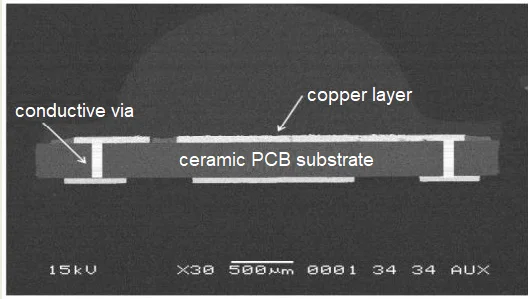
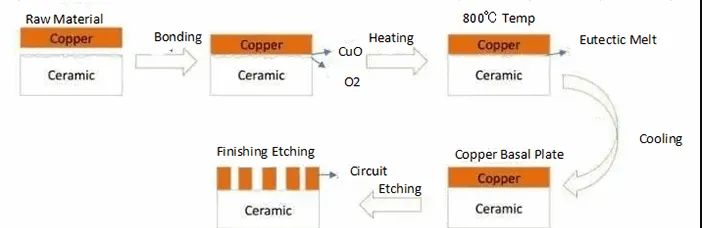
Ceramic PCB manufacturing involves distinct steps tailored to the substrate's rigidity and metallization requirements. The process begins with substrate preparation, including surface cleaning and polishing to achieve nanoscale flatness. Common metallization methods include direct bond copper (DBC), where copper foil bonds to the ceramic at high temperatures above 1000 degrees Celsius in a nitrogen atmosphere. This creates a robust eutectic bond with excellent thermal transfer. Alternative techniques like active metal brazing use titanium or zirconium to form intermetallic layers, enhancing adhesion on nitrides.
Thick-film printing deposits conductive pastes via screen printing, followed by firing at 800 to 900 degrees Celsius to sinter the layers. Thin-film sputtering offers precision for microwave circuits, depositing metals like gold or titanium-tungsten in vacuum chambers. Each method influences final properties, such as trace resolution down to 50 microns. Factories control firing profiles to prevent warpage, a common challenge due to ceramic shrinkage.
Post-metallization, vias form through laser drilling or mechanical punching, filled with conductive pastes and co-fired. Surface finishing applies nickel-gold plating for solderability and wire bondability. The entire workflow adheres to cleanliness standards to avoid contamination, which could compromise high-frequency performance.
Key Ceramic PCB Advantages
Ceramic PCB advantages stem from their inherent material properties, outperforming organics in critical areas. High thermal conductivity PCBs efficiently spread heat, maintaining junction temperatures below thresholds in power devices. This reduces the need for bulky heatsinks, enabling slimmer profiles in LED drivers and inverters. Low dielectric constant PCBs support faster signal rise times, vital for 5G base stations and radar systems.
High-temperature PCB capability allows sustained operation in automotive engine compartments or aerospace avionics, where organics would degrade. Ceramics resist oxidation and maintain integrity under thermal cycling, with expansion coefficients matching semiconductors. Electrical insulation remains stable, preventing breakdowns in high-voltage setups. These traits lower failure rates, as verified through accelerated life testing in production.
Mechanical robustness handles vibrations and shocks better, with flexural strength over 300 MPa. Hermetic sealing options protect against humidity, extending shelf life. Overall, these advantages justify the higher cost for mission-critical electronics.
Ceramic PCB Applications in High-Performance Systems
Ceramic PCB applications span sectors where reliability trumps volume production. In power electronics, they serve as substrates for IGBT modules in electric vehicles, managing kilowatts of power with minimal losses. High thermal conductivity ensures efficient cooling, supporting trends toward higher switching frequencies. RF and microwave circuits benefit from low dielectric constant PCBs, used in antennas and filters for satellite communications.
High-temperature PCBs find roles in downhole drilling tools and gas turbines, enduring 200 degrees Celsius continuously. LED lighting assemblies leverage ceramics for phosphor converters, dissipating heat from blue LEDs effectively. Aerospace hybrid circuits integrate multiple chips on ceramic bases for radar and guidance systems. Medical devices like MRI coils use them for stability under electromagnetic interference.
Emerging uses include 8K displays and quantum computing interfaces, where low loss tangents preserve signal integrity. Engineers select ceramics based on frequency, power density, and environmental factors.
Design and Manufacturing Best Practices
Designing for ceramic PCBs requires accounting for their unique traits from the outset. Layouts minimize via counts to reduce stress points, using ground planes for uniform heat spreading. Trace widths scale with current density, often 1 A per mm width for copper layers up to 300 microns thick. Simulation tools model thermal gradients, predicting hotspots before fabrication.
In manufacturing, factories implement IPC-6012E qualification to ensure performance specs for rigid boards, including ceramics. Solder mask application uses high-temp epoxies or direct polymer printing. Quality control involves X-ray inspection for voids and dye penetrant tests for cracks. Warpage measurement stays below 50 microns per side, critical for flip-chip assembly.
Multilayer stacks build via low-temp co-firing for complex interconnects. Prototyping iterates quickly with small batches, refining processes. Procurement teams specify substrate grade and metallization type upfront.
Quality Control and Reliability Assurance
Reliability hinges on stringent factory protocols. Visual and automated optical inspections detect surface defects post-firing. Electrical testing verifies continuity and insulation resistance above 100 GOhms. Thermal cycling per JEDEC J-STD-020E simulates field conditions, assessing solder joint integrity.
Shear strength tests confirm metal-ceramic bonds exceed 50 kgf/cm2. Humidity exposure checks for delamination risks. Traceability systems log every step, enabling root cause analysis. These measures align with ISO 9001:2015 for consistent quality management.
Conclusion
Ceramic PCBs unlock high-performance electronics through superior thermal, electrical, and mechanical properties. Their manufacturing demands precision but yields boards for the toughest applications. Electrical engineers benefit from ceramic PCB advantages in heat management, signal fidelity, and durability. By following best practices and standards, designs achieve optimal reliability. As electronics evolve, ceramics will remain pivotal for innovation.
FAQs
Q1: What are the main ceramic PCB advantages for high-power applications?
A1: Ceramic PCB advantages include high thermal conductivity, which dissipates heat effectively in power modules, and low CTE matching with silicon dies to prevent cracking. They support high-temperature operation without degradation, ideal for inverters and converters. Factory processes ensure uniform heat spreading, reducing thermal stress on components. Overall, they enable compact, efficient designs.
Q2: Where are ceramic PCB applications most common?
A2: Ceramic PCB applications thrive in RF microwave circuits, power electronics, and high-temperature environments like aerospace and automotive. High thermal conductivity PCBs cool LED arrays and IGBTs, while low dielectric constant variants suit 5G antennas. They excel where organics fail under heat or frequency demands.
Q3: How does high thermal conductivity PCB manufacturing differ from standard PCBs?
A3: High thermal conductivity PCB manufacturing uses DBC or AMB on aluminum nitride substrates, fired at high temperatures for strong bonds. This contrasts with FR-4 lamination, focusing on metallization adhesion rather than resin curing. Processes control shrinkage to avoid warpage, ensuring reliable heat paths.
Q4: Why choose low dielectric constant PCB for high-frequency designs?
A4: Low dielectric constant PCBs minimize signal delay and loss, supporting GHz operations in radar and telecom. Ceramics like alumina provide stable permittivity, reducing crosstalk. They maintain performance under thermal stress, unlike organics that absorb moisture.
References
IPC-6012E — Qualification and Performance Specification for Rigid Printed Boards. IPC, 2018
JEDEC J-STD-020E — Moisture/Reflow Sensitivity Classification for Nonhermetic Surface Mount Devices. JEDEC, 2014
ISO 9001:2015 — Quality Management Systems — Requirements. ISO, 2015


