 ALLPCB


Are you facing challenges with PCB assembly defects like solder bridges, solder balls, open solder joints, insufficient solder, or component misalignment? These issues can compromise the reliability and performance of your electronic devices. In this comprehensive guide, we’ll dive deep into identifying these common defects, understanding their causes, and providing actionable solutions to mitigate them. Whether you're an engineer or a manufacturer, this blog will equip you with the knowledge to improve your PCB assembly process and ensure high-quality results.
What Are PCB Assembly Defects and Why Do They Matter?
PCB assembly defects are flaws or errors that occur during the process of assembling components onto a printed circuit board (PCB). These defects can lead to functional failures, reduced product lifespan, or even complete device breakdowns. With the increasing complexity of modern electronics, even minor issues like a tiny solder bridge or a misaligned component can cause significant problems, including short circuits or signal integrity issues.
Addressing these defects is crucial for maintaining product quality, reducing manufacturing costs, and meeting customer expectations. By understanding the root causes and implementing preventive measures, you can minimize rework, improve yield rates, and ensure your PCBs perform as intended. Let’s explore some of the most common PCB assembly defects—solder bridges, solder balls, open solder joints, insufficient solder, and component misalignment—and how to tackle them effectively.
Common PCB Assembly Defects: Identification and Causes
Before diving into solutions, it’s essential to recognize what these defects look like and why they occur. Below, we break down each issue with detailed descriptions and potential causes based on industry insights.
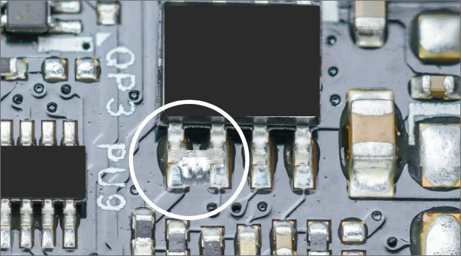
1. Solder Bridges: Unwanted Connections
Solder bridges occur when excess solder creates an unintended connection between two or more adjacent pads or leads on a PCB. This defect often results in short circuits, which can cause a device to malfunction or fail entirely. Visually, a solder bridge looks like a blob of solder spanning across pins or traces that should remain separate.
Causes:
- Excessive solder paste application during the stencil printing process.
- Improper spacing between pads or leads, especially in high-density designs.
- Inadequate reflow soldering profiles, leading to solder not settling correctly.
- Poor soldering technique during manual assembly, such as using too much solder or incorrect tip size.
Impact: Solder bridges can disrupt electrical signals, leading to unpredictable behavior or complete failure. For instance, in a high-speed circuit, a bridge might cause a signal to jump to an unintended path, resulting in data loss or corruption.
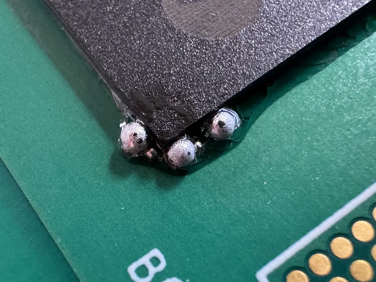
2. Solder Balls: Stray Solder Deposits
Solder balls are small, spherical solder particles that form on the PCB surface or near components during the soldering process. These stray deposits can roll around and create unintended electrical connections, posing a risk of short circuits over time.
Causes:
- Excessive moisture in the solder paste, causing it to splatter during reflow.
- Incorrect reflow temperature profiles, leading to uneven heating and solder expulsion.
- Contaminated PCB surfaces or components, which prevent proper solder adhesion.
- Improper stencil design or printing, resulting in excess paste outside the pads.
Impact: Solder balls can cause intermittent faults, especially in compact designs where they might lodge between fine-pitch components. For example, in a 0.5mm pitch BGA (Ball Grid Array) package, a stray solder ball could bridge connections, leading to signal integrity issues.
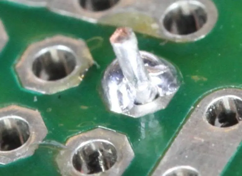
3. Open Solder Joints: Incomplete Connections
An open solder joint happens when there is no proper electrical or mechanical connection between a component lead and the PCB pad. This defect often appears as a gap or incomplete solder fillet around the lead, leading to intermittent or complete loss of connectivity.
Causes:
- Inadequate solder paste volume during printing, resulting in insufficient material for a proper joint.
- Poor component placement, where leads do not align with pads during reflow.
- Oxidation on component leads or pads, preventing solder from bonding effectively.
- Incorrect reflow profiles, such as insufficient heat to melt the solder fully.
Impact: Open solder joints can cause intermittent failures, especially under thermal or mechanical stress. For instance, a device might work initially but fail after exposure to temperature cycles (e.g., -40°C to 85°C), as the joint weakens further.
4. Insufficient Solder: Weak Joints
Insufficient solder refers to a situation where there isn’t enough solder material to form a strong, reliable joint between the component and the PCB. This defect often results in weak mechanical connections and poor electrical conductivity, visible as thin or incomplete solder fillets.
Causes:
- Under-application of solder paste during the stencil printing stage.
- Incorrect stencil aperture design, leading to reduced paste volume on pads.
- Component leads or pads with poor wettability, preventing solder from spreading properly.
- Reflow soldering issues, such as low peak temperatures (e.g., below 220°C for lead-free solder), causing incomplete melting.
Impact: Joints with insufficient solder are prone to cracking or breaking under stress, leading to reliability issues. For example, in automotive electronics, vibration can cause such joints to fail, resulting in system downtime.
5. Component Misalignment: Incorrect Placement
Component misalignment occurs when a component is not placed accurately on its designated pads during assembly. This can result in poor connections, open joints, or even short circuits if the component shifts significantly.
Causes:
- Inaccurate pick-and-place machine calibration, leading to placement errors.
- Incorrect PCB design files or Gerber data, causing misalignment during assembly setup.
- Solder paste displacement during component placement, shifting the part during reflow.
- Thermal expansion mismatches during reflow, especially with larger components.
Impact: Misaligned components can lead to functional failures or assembly rework. In high-frequency applications (e.g., 5GHz RF circuits), even a 0.1mm misalignment can alter impedance and degrade signal performance.
How to Mitigate PCB Assembly Defects
Now that we’ve identified these common defects and their causes, let’s explore practical strategies to prevent them during the PCB assembly process. These tips are designed to help engineers and manufacturers achieve higher quality and reliability.
1. Optimize Solder Paste Application
Many defects, such as solder bridges, solder balls, and insufficient solder, stem from improper solder paste application. Use a well-designed stencil with precise aperture sizes to ensure the right amount of paste is applied to each pad. Regularly inspect and clean stencils to avoid clogging or misalignment during printing. Additionally, control the environment—maintain humidity levels between 40-60% to prevent moisture-related issues in the paste that can lead to solder balls.
2. Fine-Tune Reflow Soldering Profiles
The reflow soldering process is critical to avoiding defects like open solder joints and solder bridges. Develop a reflow profile tailored to your solder paste and components, ensuring peak temperatures (e.g., 240-250°C for lead-free solder) and ramp rates are within manufacturer specifications. Use thermal profiling tools to monitor the process and ensure uniform heating across the board, preventing issues like solder ball formation or incomplete joints.
3. Enhance Component Placement Accuracy
To prevent component misalignment, calibrate pick-and-place machines regularly and verify placement accuracy with vision systems before reflow. Ensure that PCB design files are accurate and up-to-date to avoid setup errors. For high-density designs, consider using fiducial markers on the PCB to improve machine alignment precision, reducing placement errors to within 0.025mm.
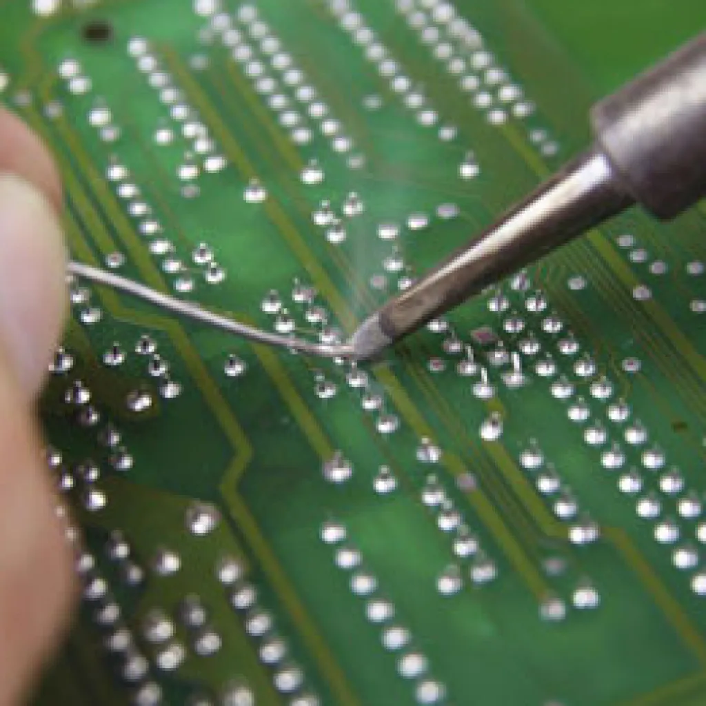
4. Conduct Thorough Inspections
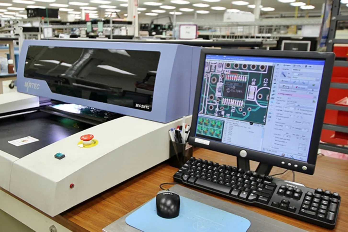
Implement automated optical inspection (AOI) systems to detect defects like solder bridges, solder balls, and misalignment immediately after reflow. AOI can identify issues with a resolution down to 0.01mm, ensuring even microscopic defects are caught early. For critical applications, complement AOI with X-ray inspection to check hidden joints, such as those under BGA packages, for open solder joints or insufficient solder.
5. Maintain Cleanliness and Quality Control
Contamination is a leading cause of defects like open solder joints and solder balls. Keep PCB surfaces, components, and assembly equipment clean to prevent oxidation or debris from interfering with soldering. Store components and boards in controlled environments to avoid moisture absorption, and use fresh solder paste within its shelf life to maintain consistent performance.
Advanced Tips for High-Reliability PCB Assembly
For applications requiring exceptional reliability, such as aerospace or medical devices, consider additional measures. Use lead-free solder alloys with higher melting points (e.g., SAC305 with a melting point of 217°C) to improve joint strength under thermal stress. Implement design-for-manufacturing (DFM) practices to ensure pad spacing and component layouts minimize the risk of solder bridges in dense areas. Finally, perform accelerated life testing (ALT) with temperature cycling (e.g., -55°C to 125°C) to validate assembly quality and identify potential weak points like insufficient solder before production ramps up.
The Importance of Partnering with Experts
While these strategies can significantly reduce PCB assembly defects, partnering with a trusted assembly service provider can take your quality to the next level. At ALLPCB, we specialize in delivering high-precision PCB assembly with rigorous quality control processes. Our advanced equipment and experienced team ensure issues like solder bridges, solder balls, open solder joints, insufficient solder, and component misalignment are minimized, providing you with reliable boards for your projects.
Conclusion: Building Better PCBs with Defect Prevention
PCB assembly defects like solder bridges, solder balls, open solder joints, insufficient solder, and component misalignment can derail your projects if left unchecked. By understanding their causes—ranging from improper solder paste application to incorrect reflow profiles—you can take proactive steps to prevent them. Optimize your processes, invest in quality inspection tools, and maintain strict cleanliness standards to achieve consistent, high-quality results.
With the actionable tips provided in this guide, you’re well-equipped to tackle these common issues and improve the reliability of your electronic assemblies. At ALLPCB, we’re committed to supporting your success with top-tier manufacturing solutions tailored to your needs. Let’s build better PCBs together by prioritizing quality at every step of the assembly process.


