 ALLPCB


Introduction
Hotspots on LED printed circuit boards represent a critical challenge in high-power lighting applications. These localized areas of elevated temperature can accelerate component degradation, reduce luminous efficacy, and trigger catastrophic failures like thermal runaway. Electric engineers must prioritize thermal management to ensure reliable performance over the product's lifecycle. Identifying hotspots on LED PCBs early through systematic diagnosis prevents costly rework and field returns. This article explores the mechanisms behind overheating, proven diagnostic techniques such as thermal imaging for LED PCBs, and actionable strategies aligned with industry best practices. By addressing these issues proactively, designs achieve optimal efficiency and longevity.
Understanding Hotspots in LED PCBs and Their Impact
Hotspots occur when heat generated by LEDs concentrates in specific board regions, exceeding safe operating limits. In LED assemblies, the primary heat source stems from the semiconductor junction within the LED package, where up to 70 percent of input power converts to thermal energy under typical conditions. Without effective dissipation, this heat builds up, causing junction temperatures to rise and initiating a feedback loop that diminishes forward voltage and increases current draw. Thermal runaway in LED lighting manifests as exponential temperature escalation, leading to phosphor degradation, color shifting, and eventual device burnout. Engineers must recognize that hotspots not only shorten lifespan but also compromise system safety in enclosed fixtures. Consistent thermal profiling during development reveals vulnerabilities before production scaling.
The relevance of hotspot management intensifies with rising LED power densities in applications like street lighting and automotive systems. Poor thermal design amplifies failure rates, with studies indicating that every 10 degree Celsius increase above optimal halves LED life expectancy. Compliance with standards like IPC-2221C ensures designs incorporate adequate thermal relief features from the outset. Neglecting these principles results in uneven light output and reliability issues that undermine product warranties. Proactive analysis maintains performance margins under varying ambient conditions and load cycles. Ultimately, mastering hotspot control elevates design quality and market competitiveness.
Causes of LED PCB Overheating
Several design and assembly factors contribute to causes of LED PCB overheating. High-power LEDs clustered too closely generate excessive localized heat, overwhelming the board's spreading capacity and creating hotspots near component pads. Inadequate copper thickness or trace widths fail to conduct heat away efficiently, as narrower paths exhibit higher thermal resistance per IPC-2152 guidelines on current-carrying capacity. Voids in solder joints or delamination under thermal stress further impede heat transfer from LED to substrate. Environmental factors, such as restricted airflow in luminaire housings, exacerbate these issues by trapping heat against the board surface.
Component selection plays a pivotal role, where LEDs with mismatched thermal resistance values overload standard FR-4 substrates lacking metal cores. Overdriven currents from improper driver circuitry push junction temperatures beyond specifications, initiating degradation cycles. Manufacturing defects like insufficient thermal vias or uneven plating thickness concentrate heat in vias or planes. Power supply fluctuations introduce dynamic loads that spike temperatures intermittently. Addressing these root causes requires holistic evaluation during layout and prototyping phases.
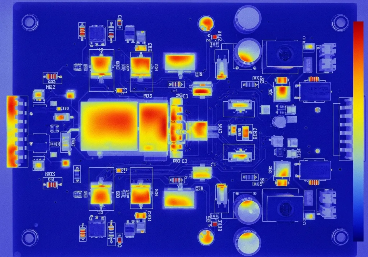
Diagnosing Hotspots: Thermal Imaging and Other Methods
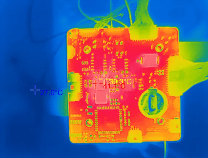
Thermal imaging for LED PCBs stands as the gold standard for identifying hotspots on LED PCBs due to its non-contact, real-time visualization. Infrared cameras capture surface temperature distributions with resolutions detecting differences as small as 0.1 degree Celsius, pinpointing anomalies like failing vias or overloaded traces. During powered operation, engineers scan assemblies under nominal and stressed conditions to map isotherms and quantify peak values. This method reveals subtle gradients invisible to visual inspection, correlating hot regions with failure modes. Complementary techniques include thermocouple arrays for precise point measurements and finite element simulations for predictive validation.
Troubleshooting begins with steady-state imaging after warm-up, followed by transient scans to capture dynamic hotspots during ramp-up. JEDEC JESD51-2A outlines environmental conditions for accurate thermal characterization, ensuring repeatability across tests. Data logging integrates with software for hotspot trending over cycles. Cross-verification with electrical measurements confirms if hotspots stem from shorts or bias issues. This multi-faceted approach accelerates root cause analysis and design iterations.
Best Practices for LED PCB Thermal Analysis and Prevention
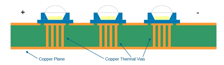
Best practices for LED PCB thermal analysis emphasize simulation-integrated design workflows. Early-stage modeling predicts hotspot formation by inputting material properties, geometries, and boundary conditions, allowing optimization before fabrication. Incorporate thermal vias arrays under LED pads, filled or plated per assembly tolerances, to channel heat to inner layers or opposite sides. Widen copper pours around high-heat components to enhance lateral spreading, guided by IPC-2152 trace heating charts. Distribute LEDs evenly, maintaining minimum spacing to avoid mutual heating effects.
Preventing thermal runaway in LED lighting demands robust heat sinking strategies. Attach aluminum or copper cores in metal-clad PCBs directly to external heatsinks via thermal interface materials, minimizing air gaps. Employ constant-current drivers to stabilize LED operation against temperature-induced voltage drops. Ventilation slots or forced convection in enclosures promote natural airflow over board surfaces. Layer stackups with dedicated ground planes act as heat spreaders, while thicker copper foils reduce via reliance. Validate prototypes through accelerated thermal cycling to expose weaknesses.
Routine monitoring post-assembly includes infrared profiling at multiple power levels. Adjust layouts iteratively based on empirical data, prioritizing edge placement for components near chassis grounding. Material choices like high-Tg laminates withstand thermal excursions without warping. These layered practices ensure compliance and field reliability.
Troubleshooting Real-World Thermal Failures
Practical troubleshooting follows a structured protocol for LED PCB assemblies exhibiting hotspots. First, power cycle under controlled current while monitoring with thermal imaging to isolate intermittent issues. Inspect for solder voids using X-ray if imaging suggests joint failures. Measure trace resistances to detect plating anomalies contributing to I2R losses. Simulate airflow with computational fluid dynamics to quantify enclosure impacts.
Common pitfalls include overlooking via stitching density, which starves inner-layer cooling. Recurring hotspots near drivers signal inadequate decoupling or grounding loops. Field returns often trace to ambient exceedances unaccounted in design margins. Document findings in a failure mode database for continuous improvement. This hands-on methodology resolves 80 percent of issues pre-production.
Conclusion
Effective troubleshooting of LED PCB hotspots hinges on understanding causes, leveraging thermal imaging for diagnosis, and implementing rigorous prevention measures. From distributed layouts and thermal vias to standards-compliant analysis, these strategies mitigate overheating risks comprehensively. Electric engineers benefit from integrating simulation, prototyping, and empirical testing throughout the design cycle. Prioritizing thermal management not only prevents failures but enhances overall system efficiency and lifespan. Adopt these best practices to deliver robust LED lighting solutions that perform reliably in demanding environments.
FAQs
Q1: What are the primary causes of LED PCB overheating?
A1: Causes of LED PCB overheating include clustered high-power components, insufficient thermal vias, thin copper traces, and poor airflow in enclosures. These factors concentrate heat from LED junctions, raising surface temperatures and risking degradation. Inadequate heatsinking or solder defects further impede dissipation. Addressing them through layout optimization and material selection maintains safe operating margins. Early identification via thermal profiling prevents escalation to thermal runaway.
Q2: How does thermal imaging help in identifying hotspots on LED PCBs?
A2: Thermal imaging for LED PCBs visualizes temperature distributions non-invasively, detecting hotspots with high spatial resolution during operation. It reveals patterns like via failures or trace overloads invisible otherwise. Scans under load correlate hot zones with electrical faults. This method supports rapid prototyping iterations and quality control. Combined with standards like JEDEC JESD51-2A, it ensures accurate, repeatable diagnostics for reliable designs.
Q3: What are best practices for preventing thermal runaway in LED lighting?
A3: Preventing thermal runaway in LED lighting involves constant-current drivers, metal-core substrates, and thermal vias arrays. Distribute heat sources evenly and maximize copper planes for spreading. Validate with infrared analysis and simulations. Enclosure designs promoting convection enhance dissipation. These measures keep junction temperatures below critical thresholds, extending lifespan and efficacy.
Q4: How can engineers perform effective LED PCB thermal analysis?
A4: Best practices for LED PCB thermal analysis start with IPC-2221C-guided layouts, followed by finite element modeling and prototype infrared scanning. Measure theta values per JEDEC protocols under varied conditions. Optimize vias, planes, and sinks iteratively. Document hotspots and refine stackups accordingly. This systematic approach minimizes risks and ensures production scalability.
References
IPC-2221C — Generic Standard on Printed Board Design. IPC, 2023
IPC-2152 — Standard for Determining Current Carrying Capacity in Printed Board Design. IPC, 2009
JEDEC JESD51-2A — Integrated Circuits Thermal Test Method Environmental Conditions - Natural Convection. JEDEC, 2008


