ALLPCB


If you're facing challenges with copper cladding in PCB manufacturing, such as delamination, etching problems, or shorts, you're not alone. These issues can lead to defective boards, increased costs, and delays in production. The good news? Most copper cladding problems can be identified and resolved with the right troubleshooting steps. In this guide, we'll walk you through common defects like copper cladding delamination, etching issues, and shorts, offering practical solutions to ensure high-quality PCB production.
Understanding Copper Cladding in PCB Manufacturing
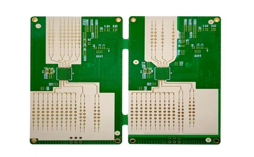
Copper cladding is a critical component in printed circuit boards (PCBs). It forms the conductive pathways that connect components, ensuring electrical signals flow smoothly. Typically, copper foil is laminated onto a substrate material, like FR-4, during the manufacturing process. The thickness of this copper layer often ranges from 0.5 oz/ft2 to 2 oz/ft2 (approximately 17 to 70 micrometers), depending on the board's design and application.
While copper cladding is essential for functionality, it’s also prone to defects during manufacturing. Issues like delamination, uneven etching, and electrical shorts can compromise the board's performance. Understanding these problems and how to troubleshoot them is key to producing reliable PCBs.
Common Copper Cladding Issues in PCB Manufacturing
Let’s dive into the most frequent copper cladding defects encountered during PCB production. By identifying these issues early, you can take corrective actions to minimize waste and improve yield.
1. Copper Cladding Delamination
Copper cladding delamination occurs when the copper layer separates from the substrate material. This defect can lead to poor electrical connectivity and mechanical failure. Delamination often appears as blisters or peeling on the board’s surface and is typically caused by:
- Moisture Absorption: Excess humidity during storage or assembly can weaken the bond between copper and substrate.
- Thermal Stress: Repeated exposure to high temperatures during soldering (often above 260°C) can cause the layers to expand and contract at different rates, leading to separation.
- Poor Material Quality: Low-grade substrates or adhesives may fail to bond properly with the copper foil.
Troubleshooting Tip: To prevent copper cladding delamination, ensure proper storage conditions with humidity levels below 50%. Use high-quality materials that meet industry standards, and control thermal profiles during soldering to avoid exceeding the glass transition temperature (Tg) of the substrate, typically around 130-170°C for FR-4 materials.
2. Copper Cladding Etching Problems
Etching is the process of removing unwanted copper from the board to create the desired circuit pattern. However, issues during etching can result in defective traces or pads. Common copper cladding etching problems include:
- Over-Etching: Excessive removal of copper, leading to thinner traces than designed. This can increase resistance and affect signal integrity, especially in high-frequency applications where trace impedance might deviate from the target (e.g., 50 ohms).
- Under-Etching: Insufficient copper removal, causing unwanted connections or shorts between traces.
- Uneven Etching: Variations in etching depth across the board, often due to inconsistent etchant concentration or spray pressure.
Troubleshooting Tip: Monitor etchant chemistry closely, maintaining consistent concentrations (e.g., 2-3% hydrochloric acid in ferric chloride solutions). Adjust spray pressure and conveyor speed during the etching process to ensure uniformity. Regularly inspect equipment for clogs or wear that could disrupt the process.
3. Copper Cladding Shorts
Short circuits in copper cladding occur when unintended connections form between traces or pads, often due to manufacturing defects. These shorts can cause electrical failures, overheating, or complete board malfunction. Common causes include:
- Residual Copper: Leftover copper from incomplete etching creates bridges between traces.
- Solder Mask Issues: Poor application of solder mask can expose copper areas, leading to accidental contact during assembly.
- Design Errors: Insufficient spacing between traces (often less than 0.1 mm in high-density designs) increases the risk of shorts.
Troubleshooting Tip: Use automated optical inspection (AOI) systems to detect residual copper or solder mask defects early in the process. Ensure design rules account for minimum trace spacing based on manufacturing capabilities, typically 0.15 mm or more for standard processes.
4. Other PCB Manufacturing Defects Related to Copper Cladding
Beyond the primary issues of delamination, etching problems, and shorts, other defects can also arise during PCB manufacturing. These include:
- Plating Voids: Incomplete copper plating in vias or through-holes, leading to weak connections. This often results from poor cleaning before plating or inconsistent current density during electroplating (ideal range: 1-3 A/dm2).
- Pad Lifting: Copper pads detaching from the substrate during soldering or rework, often due to thermal stress or inadequate adhesion.
Troubleshooting Tip: For plating voids, ensure thorough cleaning and activation of surfaces before plating. For pad lifting, optimize soldering temperatures (e.g., peak reflow at 245°C for lead-free solder) and use substrates with higher thermal resistance.
Step-by-Step Guide to Troubleshooting Copper Cladding Issues
Now that we’ve covered the common defects, let’s walk through a systematic approach to troubleshoot and resolve copper cladding issues in PCB manufacturing. Follow these steps to identify root causes and implement effective solutions.
Step 1: Visual Inspection
Start by examining the PCB for visible defects. Use a magnifying glass or microscope to check for signs of delamination, uneven etching, or shorts. Look for blisters, peeling, or discoloration that might indicate thermal or moisture-related issues.
Step 2: Electrical Testing
Perform continuity and isolation tests using a multimeter or automated test equipment. Check for shorts between traces or open circuits where connections should exist. Measure trace resistance to ensure it matches design specifications (e.g., less than 0.1 ohms for a typical power trace).
Step 3: Process Review
Analyze the manufacturing process to pinpoint potential causes. Review parameters like etchant concentration, lamination pressure (typically 200-300 psi), and soldering temperatures. Compare these against recommended values to identify deviations.
Step 4: Material Assessment
Evaluate the quality of raw materials, including copper foil and substrate. Ensure they meet industry standards, such as IPC-4562 for copper foil, which specifies purity and thickness tolerances. Poor material quality often contributes to defects like delamination or pad lifting.
Step 5: Implement Corrective Actions
Based on your findings, take corrective measures. For example, if over-etching is the issue, adjust the etching time or etchant strength. If delamination is caused by moisture, improve storage conditions and consider baking the boards at 120°C for 2-4 hours before assembly to remove trapped humidity.
Preventive Measures for Copper Cladding Defects
While troubleshooting is essential, preventing copper cladding issues in the first place is even better. Here are some proactive steps to minimize defects during PCB manufacturing.
- Design Optimization: Use design software to simulate thermal and electrical performance, ensuring trace widths and spacing meet manufacturing tolerances (e.g., minimum 0.2 mm spacing for 1 oz copper).
- Quality Control: Implement strict quality checks at every stage, from incoming material inspection to final testing. Use tools like X-ray inspection to detect hidden delamination or voids.
- Process Consistency: Standardize manufacturing parameters, such as lamination temperature (around 180-200°C) and etching duration, to reduce variability.
- Environmental Control: Maintain a clean, humidity-controlled environment (30-50% relative humidity) to prevent moisture-related issues.
Why Addressing Copper Cladding Issues Matters
Copper cladding defects can have serious consequences for PCB performance and reliability. Delamination can lead to mechanical failure, while etching problems and shorts can cause signal loss or complete circuit failure. In high-stakes applications, such as medical devices or aerospace systems, these issues could even pose safety risks.
By troubleshooting and preventing copper cladding issues, you ensure better product quality, reduce production costs, and improve customer satisfaction. A single defective board might cost only a few dollars to replace, but in large-scale production, these costs can quickly add up to thousands if not addressed.
Conclusion
Copper cladding issues in PCB manufacturing, such as delamination, etching problems, and shorts, are common but manageable challenges. By understanding the root causes of these defects and following a structured troubleshooting approach, you can minimize their impact on your production process. Implementing preventive measures, like optimizing design and controlling environmental conditions, further ensures consistent quality.
Whether you’re dealing with copper cladding delamination or etching inconsistencies, the key is to act quickly and systematically. With the practical tips and steps outlined in this guide, you’re well-equipped to tackle these PCB manufacturing defects and achieve reliable, high-performing boards for your projects.