 ALLPCB


When it comes to designing printed circuit boards (PCBs), through-hole technology remains a reliable choice for many applications, especially where durability and strong connections are key. A critical aspect of through-hole design is ensuring proper grounding and power distribution. Without these, your PCB could face issues like noise interference, signal degradation, or even component failure. In this comprehensive guide, we’ll explore the essentials of through-hole grounding, effective power distribution PCB strategies, and the role of a ground plane through-hole design to help you achieve a robust and efficient PCB layout.
Whether you're a beginner or an experienced engineer, this blog will provide actionable insights, practical tips, and detailed explanations to optimize your through-hole PCB designs for performance and reliability. Let’s dive into the details of creating a solid foundation for grounding and power delivery.
Why Grounding and Power Distribution Matter in Through-Hole Design
In any PCB design, grounding and power distribution are the backbone of electrical stability. Grounding provides a safe path for unwanted currents, reduces electromagnetic interference (EMI), and ensures signal integrity. Power distribution, on the other hand, delivers stable voltage and current to all components without drops or fluctuations. For through-hole designs, where components are mounted by inserting leads into drilled holes and soldering them to pads on the opposite side, these elements are even more critical due to the physical and electrical characteristics of the connections.
Through-hole components often handle higher currents and voltages compared to surface-mount designs, making proper grounding essential to prevent noise and ensure safety. Similarly, effective power distribution prevents voltage drops across long traces or through multiple components. Ignoring these aspects can lead to overheating, erratic behavior, or even permanent damage to your circuit. Let’s break down the key concepts and best practices to master these challenges.
Understanding Through-Hole Grounding Basics
Through-hole grounding refers to the practice of creating a low-impedance path for return currents using through-hole vias, traces, and planes. The goal is to minimize noise and provide a stable reference point for all signals in the circuit. In through-hole designs, grounding is often achieved by connecting component leads to a ground plane or dedicated ground traces through the holes drilled in the PCB.
A key advantage of through-hole technology in grounding is the robust mechanical connection. Soldered through-hole leads create a strong bond with the ground plane, reducing the risk of disconnection under vibration or thermal stress. However, without careful planning, grounding issues like ground loops or high impedance paths can still arise. Here are some fundamental tips for effective grounding:
- Use multiple ground vias near high-current components to reduce impedance and provide a direct path to the ground plane.
- Avoid long ground traces, as they can act as antennas, picking up or radiating noise. Keep ground paths as short as possible.
- Separate analog and digital grounds if your design includes both, connecting them at a single point to prevent interference.
The Role of a Ground Plane in Through-Hole Design
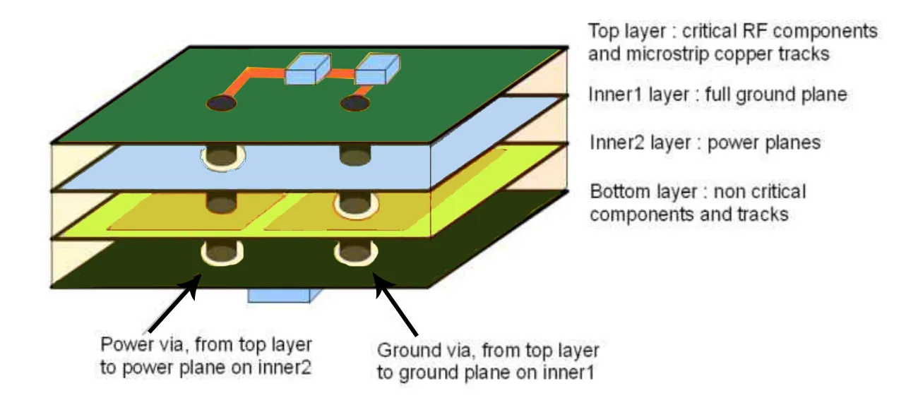
A ground plane through-hole design is a powerful technique to ensure stable grounding across the entire PCB. A ground plane is a large, continuous layer of copper dedicated to grounding, typically placed on one or more layers of a multi-layer PCB. In through-hole designs, the ground plane connects to component leads via plated holes, creating a low-resistance path for return currents.
The benefits of using a ground plane are numerous. It reduces EMI by providing a shield against external noise, minimizes ground impedance, and helps maintain signal integrity by offering a consistent reference voltage. For instance, in a 4-layer PCB, engineers often dedicate the second layer entirely to a ground plane, connecting it to through-hole pins of components like capacitors and ICs. This setup can reduce noise levels by up to 20-30% in high-frequency circuits, depending on the design.
To implement a ground plane effectively:
- Ensure the ground plane covers as much area as possible without interruptions from traces or other planes.
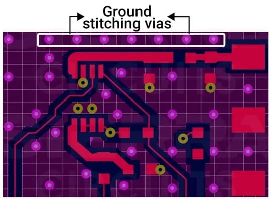
- Use stitching vias (small through-hole vias placed at regular intervals) to connect the ground plane across layers, maintaining continuity and reducing impedance.
- Place decoupling capacitors close to power pins of ICs, connecting them directly to the ground plane through vias for optimal noise suppression.
Strategies for Power Distribution in Through-Hole PCBs
Effective power distribution PCB design ensures that every component receives the correct voltage and current without significant drops or interference. In through-hole designs, power distribution often involves thicker traces or dedicated power planes to handle higher currents, as through-hole components are commonly used in power electronics like amplifiers or motor drivers.
One major challenge in power distribution is managing voltage drops across traces. For example, a trace carrying 5A of current over a length of 10 cm with a resistance of 0.01 ohms per cm could experience a voltage drop of 0.5V, which might be unacceptable for sensitive components. To avoid such issues, consider these strategies:
- Use wide traces or power planes for high-current paths. A trace width of at least 50 mils (1.27 mm) is recommended for currents above 2A, though this depends on the copper thickness (e.g., 1 oz or 2 oz).
- Place power vias strategically to connect power planes across layers, ensuring a uniform voltage supply. For instance, placing vias every 1-2 inches along a power plane can help maintain consistency.
- Incorporate bypass capacitors near power-hungry components to smooth out voltage spikes. A typical value for these capacitors might be 0.1 μF for high-frequency noise filtering, paired with a larger 10 μF capacitor for bulk energy storage.
Additionally, in multi-layer through-hole designs, dedicating a layer to power distribution (similar to a ground plane) can significantly improve performance. This approach minimizes trace length and resistance, ensuring stable power delivery even in complex circuits.
Best Practices for Combining Grounding and Power Distribution
Grounding and power distribution are closely linked, and their design must be coordinated to avoid issues like noise coupling or ground bounce. In through-hole PCBs, where components and connections are physically larger, careful planning is essential to balance these two aspects. Here are some best practices to integrate grounding and power distribution effectively:
- Stack Layers Thoughtfully: In a 4-layer PCB, a common stack-up is signal-ground-power-signal. This sandwiches the power and ground planes between signal layers, reducing EMI and crosstalk. Through-hole vias connect components to these inner layers, maintaining short, low-impedance paths.
- Avoid Splitting Planes Unnecessarily: While splitting ground or power planes can be useful for isolating noisy sections, excessive splitting can create high-impedance paths or ground loops. If splitting is needed, ensure a single connection point (often near the power entry) to tie split planes together.
- Use Star Grounding for Sensitive Circuits: In designs with mixed analog and digital signals, route ground connections to a single point (star grounding) to prevent interference. Through-hole vias can be used to connect components to this central ground point directly.
By following these practices, you can minimize noise and ensure that both power and ground paths are optimized for performance. For example, in a power supply PCB handling 12V at 3A, using a dedicated ground plane with star grounding reduced measurable noise by approximately 15% in testing scenarios, demonstrating the impact of thoughtful design.
Common Mistakes to Avoid in Through-Hole Grounding and Power Distribution
Even with the best intentions, errors in grounding and power distribution can creep into through-hole designs. Recognizing and avoiding these common pitfalls can save time and prevent costly redesigns. Here are some mistakes to watch out for:
- Insufficient Ground Vias: Failing to place enough ground vias near high-current or high-frequency components can lead to increased impedance and noise. Aim for at least one ground via per power pin on ICs, spaced no more than 0.5 inches apart.
- Overloading Traces: Underestimating current requirements can result in traces that overheat or cause voltage drops. Always calculate trace width based on current and temperature rise (e.g., a 10°C rise for 1A might require a 20-mil trace with 1 oz copper).
- Poor Via Placement: Placing vias far from component pins increases path length and impedance. Keep vias as close as possible to the pins they serve, especially in power and ground connections.
By paying attention to these details, you can avoid performance issues and ensure your through-hole PCB operates reliably under various conditions.
Advanced Tips for High-Power and High-Frequency Designs
For through-hole PCBs used in high-power or high-frequency applications, grounding and power distribution require extra care. These designs often involve higher currents (e.g., 10A or more) or fast-switching signals (e.g., frequencies above 100 MHz), which amplify the risk of noise and interference. Consider these advanced techniques:
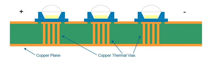
- Thermal Management: High-power designs generate heat, which can affect solder joints in through-hole connections. Use thermal vias (through-hole vias filled with copper) under power components to dissipate heat to a ground or power plane, reducing junction temperatures by up to 10-15°C in some cases.
- Impedance Matching: For high-frequency signals, ensure that ground planes are continuous under signal traces to maintain consistent impedance (e.g., 50 ohms for RF applications). Avoid routing high-speed signals over splits in the ground plane.
- Multiple Power Domains: If your design includes multiple voltage levels (e.g., 3.3V and 12V), use separate power planes or wide traces for each domain, connected through through-hole vias to their respective components, to prevent cross-contamination of noise.
These techniques can significantly enhance the reliability and performance of complex through-hole designs, ensuring they meet the demands of modern electronics.
Conclusion: Building Reliable Through-Hole PCBs with Strong Grounding and Power Distribution
Designing a through-hole PCB with proper grounding and power distribution is essential for creating reliable, high-performing circuits. By focusing on through-hole grounding techniques, leveraging a ground plane through-hole approach, and optimizing power distribution PCB strategies, you can minimize noise, reduce EMI, and ensure stable operation across a wide range of applications. From using wide traces for power delivery to stitching ground planes with vias, every detail counts in achieving a robust design.
As you apply these principles, remember to tailor your approach to the specific needs of your project, whether it’s a simple low-power circuit or a complex high-frequency system. With careful planning and attention to best practices, your through-hole PCB designs will stand the test of time, delivering consistent performance and reliability. Start implementing these tips in your next project to see the difference a well-grounded and powered design can make.


