 ALLPCB


If you're new to designing printed circuit boards (PCBs) and wondering how to master PCB trace routing, you're in the right place. Trace routing is the process of creating paths on your PCB to connect components electrically. For beginners, it can seem tricky, but with the right techniques, tools like KiCad and Eagle, and a mix of manual routing and autorouting, you can create a functional design for your first project. In this tutorial, we'll walk you through the basics of PCB routing, from understanding traces and connections to easy, actionable steps for success.
This guide is tailored for beginners, breaking down complex ideas into simple, practical tips. We'll cover everything you need to know about routing traces, placing components, and ensuring your connections are reliable. Let's dive into the world of PCB design with clear techniques to help you succeed on your first project.
What Is PCB Trace Routing and Why Does It Matter?
PCB trace routing is the process of drawing conductive paths, or "traces," on a circuit board to connect components like resistors, capacitors, and integrated circuits. These traces act like wires, carrying electrical signals or power between parts of your design. Proper routing ensures your circuit works as intended, while poor routing can lead to signal interference, overheating, or even a non-functional board.
For beginners, understanding the importance of trace routing is key. A well-routed PCB minimizes electrical noise, reduces the risk of short circuits, and makes your design more efficient. Whether you're using manual routing for precision or autorouting for speed, mastering this skill is essential for any PCB project. Let's explore the basics to get you started.
Key Concepts in PCB Trace Routing for Beginners
Before jumping into the tools and techniques, it's helpful to understand a few core ideas about PCB routing. These concepts will guide your decisions as you design your first board.
- Traces: These are the copper paths on your PCB that carry electrical signals or power. Their width and length affect how much current they can handle and how signals behave.
- Connections: These refer to how components are linked via traces. Good connections ensure reliable performance, while poor ones can cause failures.
- Components: These are the physical parts on your PCB, like LEDs or microcontrollers. Their placement affects how traces are routed.
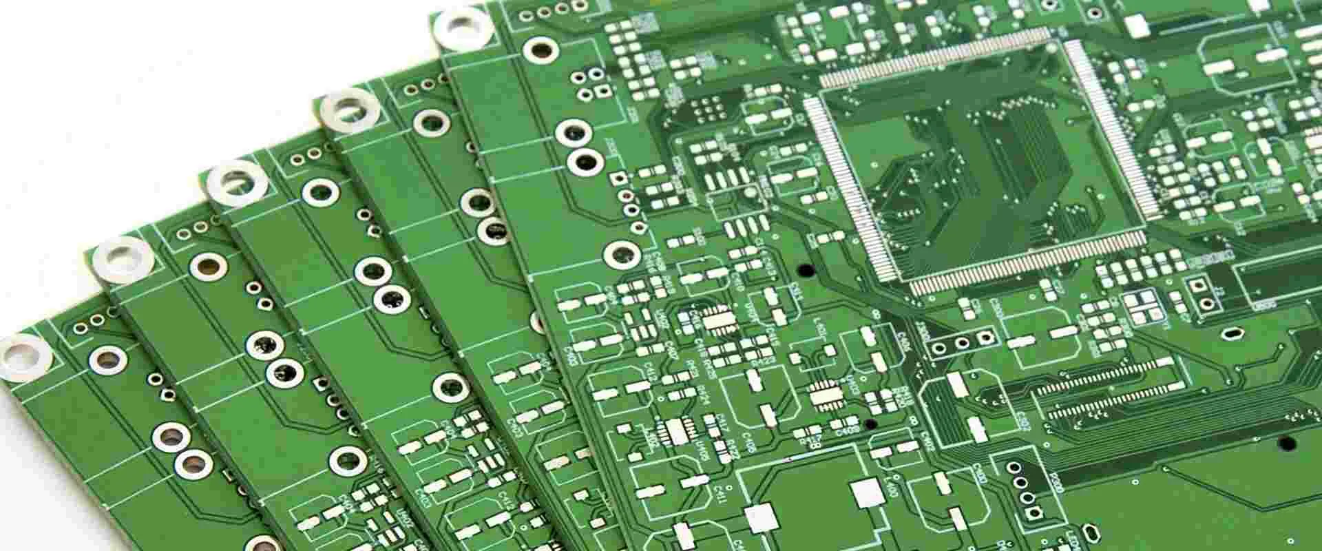
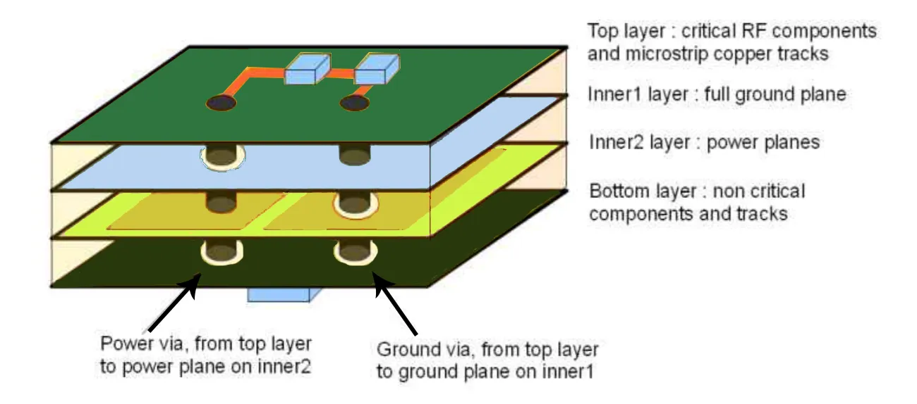
- Layers: PCBs can have multiple layers (e.g., 2-layer or 4-layer boards). Beginners often start with 2-layer boards, routing traces on the top and bottom.
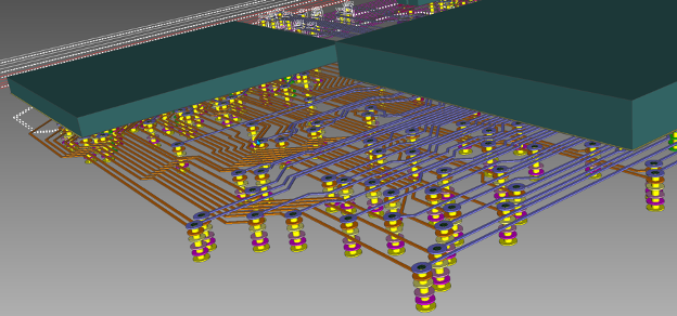
- Vias: These are small holes that connect traces between layers. They’re crucial for multi-layer designs or when space is tight.
With these basics in mind, let's look at how to approach routing for your first project.
Step-by-Step Guide to PCB Trace Routing
Routing traces for your first PCB project doesn't have to be overwhelming. Follow these easy steps to create a clean and functional design. We'll focus on techniques that work whether you're using manual routing or autorouting in tools like KiCad or Eagle.
Step 1: Plan Your Component Placement
Before routing any traces, arrange your components on the board. Good placement reduces the length of traces and minimizes crossing paths, making routing easier. Place components logically—group related parts together, like keeping power supply components near each other. Also, consider the physical size of components to avoid overcrowding.
For example, if you're designing a simple LED circuit, place the microcontroller near the LEDs to keep signal traces short. Shorter traces (e.g., under 10 mm for high-speed signals) help reduce signal delay and interference. Start with a rough layout, then refine it as you route.
Step 2: Define Your Design Rules
Design rules set the limits for trace width, spacing, and other parameters. For beginners, stick to standard values. A common trace width for low-current signals is 0.25 mm (10 mils), while power traces might need 0.5 mm (20 mils) or more to handle higher currents (e.g., 1-2 amps). Spacing between traces should be at least 0.2 mm (8 mils) to prevent short circuits.
Most PCB design software, like KiCad and Eagle, lets you set these rules before routing. This ensures your traces meet manufacturing requirements and perform reliably.
Step 3: Start with Power and Ground Traces
Route power and ground traces first. These are critical for providing stable voltage to your components. Use wider traces for power (e.g., 0.5-1 mm) to handle current without overheating. Many beginners create a "ground plane"—a large copper area on one layer dedicated to ground—to reduce noise and simplify connections.
For a 2-layer board, place the ground plane on the bottom layer and route signal traces on top. This setup helps shield signals from interference, especially for designs with frequencies above 1 MHz.
Step 4: Route Critical Signals Manually
For important connections, like high-speed signals (e.g., USB or clock lines running at 10 MHz or more), use manual routing. Manual routing gives you full control over trace paths, avoiding sharp corners that can cause signal reflection. Aim for 45-degree angles instead of 90-degree turns to maintain signal integrity.
In tools like KiCad, press the 'X' key to start routing a trace manually. Click to set points along the path, and the software will highlight the net (connection) you're working on. In Eagle, use the "Route" tool to draw traces with precision. Take your time with critical signals—rushing can lead to errors.
Step 5: Use Autorouting for Simpler Connections
Autorouting is a time-saver for non-critical traces. Both KiCad and Eagle offer autorouting features or support external plugins for this purpose. Autorouting automatically connects components based on your design rules, but it’s not always perfect. It might create long, inefficient paths or miss optimal layouts.
For your first project, use autorouting for basic connections (e.g., low-speed signals under 100 kHz), then review and adjust the traces manually. This hybrid approach balances speed and accuracy. In KiCad, you can access autorouting via third-party tools, while Eagle has a built-in autorouter under the "Tools" menu.
Step 6: Check for Errors and Optimize
After routing, run a design rule check (DRC) in your software to spot errors like unconnected pins or traces too close together. KiCad and Eagle both offer DRC tools that highlight issues in red or with error messages. Fix any problems by rerouting traces or adjusting component placement.
Also, look for ways to optimize your design. Can you shorten a trace to reduce resistance? Are there unnecessary vias that add cost? A clean layout not only works better but also looks professional.
Choosing the Right Tool: KiCad vs. Eagle for Beginners
When starting with PCB routing, the software you choose can make a big difference. Two popular options for beginners are KiCad and Eagle. Both are powerful, but they cater to slightly different needs. Here's a quick comparison to help you decide.
KiCad: Free and Open-Source
KiCad is a free, open-source tool perfect for beginners on a budget. It offers a full suite of features for schematic capture and PCB layout, including manual routing and support for autorouting via external plugins. Its user interface is straightforward, though it may feel less polished than paid software.
KiCad is ideal if you're working on hobby projects or learning PCB design. It supports 2-layer to multi-layer boards and has a large community for tutorials and support. For trace routing, its interactive router helps guide traces manually with real-time feedback.
Eagle: User-Friendly with a Free Tier
Eagle offers a free version with limitations (e.g., smaller board size and 2-layer maximum), but it's still a great choice for beginners. Its interface is intuitive, and the built-in autorouter is handy for quick layouts. Eagle also integrates well with larger design ecosystems if you upgrade to a paid plan.
For first-time PCB designers, Eagle's ease of use makes routing traces less daunting. Its "Route" tool and autorouter simplify connecting components, though manual adjustments are often needed for optimal results.
Both tools are excellent for learning PCB routing. Pick KiCad if you want a free, unlimited option, or Eagle if you prefer a polished interface with a free tier for small projects.
Common Mistakes in PCB Trace Routing and How to Avoid Them
As a beginner, it's easy to make mistakes when routing traces. Here are some common pitfalls and tips to avoid them.
- Overlapping Traces: Traces too close together can cause shorts. Always maintain spacing (e.g., 0.2 mm or more) and use DRC to catch errors.
- Long Signal Paths: Long traces for high-speed signals (above 1 MHz) can introduce noise. Keep critical traces short and direct.
- Ignoring Power Needs: Thin traces for power lines can overheat. Use wider traces (e.g., 0.5 mm) for currents over 500 mA.
- Sharp Corners: 90-degree bends in traces can disrupt high-speed signals. Use 45-degree angles or curves instead.
By paying attention to these details, you'll create a more reliable PCB design on your first try.
Advanced Tips for Better PCB Routing
Once you're comfortable with the basics, try these advanced techniques to improve your designs.
- Differential Pairs: For high-speed signals like USB, route traces as differential pairs with equal lengths to maintain timing. KiCad offers tools to set this up under net class settings.
- Impedance Matching: For signals at 50 ohms (common for RF designs), adjust trace width and spacing using online calculators. A typical 50-ohm trace on a 1.6 mm board might be 0.3 mm wide.
- Via Stitching: Add multiple vias around ground planes to improve shielding and reduce noise, especially for designs above 10 MHz.
These tips aren't necessary for every project, but they can elevate your skills as you gain experience.
Conclusion: Start Routing with Confidence
PCB trace routing might seem complex at first, but with these simple techniques, you're ready to tackle your first project. Start by planning your component placement, setting design rules, and routing power traces. Use manual routing for critical connections and autorouting for simpler ones, whether you're in KiCad or Eagle. Always check your work with a DRC to catch errors early.
By following this beginner tutorial, you'll build a solid foundation in PCB routing. Focus on clean, efficient trace paths to ensure your connections are reliable and your components work as intended. With practice, you'll gain the confidence to design more complex boards. Grab your tools, start small, and enjoy the process of creating something functional from scratch.


