In the fast-paced world of electronics, ensuring signal integrity in high-speed circuits is more critical than ever. One of the key factors in achieving this is controlled impedance in PCB design. But what exactly is controlled impedance, and why does it matter? Simply put, controlled impedance refers to the careful management of a PCB trace's resistance to alternating signals, ensuring that high-frequency signals travel without distortion or loss. This guide dives deep into the secrets of impedance control, covering essential topics like controlled impedance PCB manufacturing, impedance matching techniques, microstrip vs stripline impedance, impedance control in differential pairs, and impedance testing methods. Whether you're an engineer or a designer, this comprehensive resource will equip you with the knowledge to master PCB design for high-performance applications.
Why Controlled Impedance Matters in PCB Design
In modern electronics, devices operate at increasingly higher frequencies, often in the gigahertz (GHz) range. At these speeds, even small mismatches in impedance can cause signal reflections, crosstalk, or data loss, leading to system failures. Controlled impedance ensures that the electrical characteristics of PCB traces match the requirements of the signals they carry. This is especially important in applications like telecommunications, automotive systems, and high-speed computing, where signal integrity directly impacts performance.
By maintaining a consistent impedance—often specified as 50 ohms for single-ended signals or 100 ohms for differential pairs—designers can minimize signal distortion and ensure reliable operation. Let’s explore how this is achieved through various design and manufacturing techniques.
Understanding the Basics of Controlled Impedance
Controlled impedance is the characteristic impedance of a PCB trace, determined by factors like trace width, thickness, spacing, and the dielectric properties of the board material. It is typically measured in ohms and must match the impedance of the connected components or transmission lines to avoid signal reflections.
For example, a common single-ended trace might be designed for 50 ohms, a standard value for many high-frequency applications. If the impedance deviates—say, to 60 ohms due to manufacturing variations—reflections can occur, degrading signal quality. Achieving controlled impedance starts with precise design and continues through careful manufacturing processes.
Factors Affecting Impedance in PCB Design
- Trace Width and Thickness: Wider traces generally have lower impedance, while thinner traces have higher impedance. For a 50-ohm trace on a standard FR-4 material, a width of about 6 mils (0.006 inches) might be needed, depending on the layer stack-up.
- Dielectric Constant (Dk): The material of the PCB, such as FR-4 with a Dk of around 4.2-4.5, influences impedance. High-frequency designs often use materials with lower Dk values for better control.
- Trace Spacing: The distance between a trace and its reference plane (ground or power) affects impedance. Closer spacing lowers impedance.
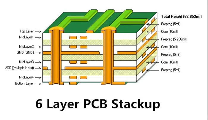
- Layer Stack-Up: The arrangement of copper and dielectric layers in a multilayer PCB impacts how signals behave, requiring careful planning for impedance control.
Controlled Impedance PCB Manufacturing: Key Considerations
When it comes to controlled impedance PCB manufacturing, precision is everything. Manufacturers must adhere to tight tolerances to ensure that the final board matches the designer’s specifications. This involves selecting the right materials, maintaining consistent trace dimensions, and using advanced fabrication techniques.
For instance, during the etching process, over- or under-etching can alter trace widths by as little as 0.5 mils, significantly affecting impedance. To counter this, manufacturers often use impedance calculators and simulation tools to predict outcomes and adjust processes accordingly. Additionally, they may perform post-production testing to verify that impedance values fall within the specified range, typically ±10% of the target (e.g., 50 ohms ±5 ohms).
Collaboration between designers and manufacturers is crucial. Designers should provide detailed stack-up information and impedance requirements in their design files, while manufacturers must communicate any limitations or adjustments needed during production.
Impedance Matching Techniques for Optimal Signal Integrity
One of the core goals of controlled impedance design is impedance matching—ensuring that the impedance of a trace matches that of the source and load. Poor matching can lead to signal reflections, where part of the signal bounces back, causing interference. Let’s look at some effective impedance matching techniques used in PCB design.
1. Proper Trace Routing
Routing traces with consistent width and avoiding abrupt changes in direction helps maintain uniform impedance. For high-speed signals, designers often use 45-degree angles or curved traces instead of sharp 90-degree bends to minimize reflections.
2. Termination Resistors
In some cases, adding termination resistors at the end of a transmission line can absorb reflected signals. For a 50-ohm line, a 50-ohm resistor placed at the load end can effectively match impedance and prevent reflections.
3. Use of Simulation Tools
Before fabrication, designers can use software to simulate signal behavior and calculate impedance. These tools account for variables like trace geometry and material properties, helping to fine-tune the design for perfect matching.
Microstrip vs Stripline Impedance: Which Is Right for Your Design?
When designing for controlled impedance, one key decision is choosing between microstrip and stripline configurations. Both are types of transmission lines used in PCBs, but they differ in structure and performance. Let’s compare microstrip vs stripline impedance to help you decide.
Microstrip Overview
Microstrip traces are located on the outer layers of a PCB, with a ground plane directly below them. This configuration is easier to manufacture and allows for simpler impedance calculations. For example, a microstrip trace on FR-4 material might achieve 50 ohms with a width of 6 mils and a dielectric height of 5 mils.
However, microstrips are more susceptible to electromagnetic interference (EMI) since they are exposed on the surface. They are best suited for simpler designs or when cost is a concern.
Stripline Overview
Stripline traces are embedded between two ground planes within the PCB, offering better shielding from EMI. This makes them ideal for high-frequency applications where signal integrity is paramount. Achieving 50 ohms in a stripline might require a slightly different trace width, often narrower due to the dual reference planes.
The downside is that striplines are more complex to manufacture and test, as they are internal to the board. They are typically used in multilayer designs for critical signals.
Key Difference: Microstrip is cost-effective and easier to adjust, while stripline provides superior noise immunity at the cost of complexity. Choose based on your project’s frequency, EMI requirements, and budget.
Impedance Control in Differential Pairs: A Must for High-Speed Signals
In high-speed digital designs, differential pairs are commonly used to transmit data with reduced noise. These pairs consist of two traces carrying complementary signals, and their impedance must be carefully controlled. Let’s explore impedance control in differential pairs.
Differential impedance, often targeted at 100 ohms for standards like USB or Ethernet, depends on the spacing between the two traces and their individual characteristic impedance. For instance, two traces each with 50 ohms characteristic impedance might need a specific spacing (e.g., 8 mils) to achieve a 100-ohm differential impedance.
Key design tips include:
- Equal Length Routing: Ensure both traces in the pair are of equal length to avoid signal skew, which can disrupt timing.
- Consistent Spacing: Maintain uniform spacing between the traces to keep differential impedance stable.
- Ground Plane Reference: Place a continuous ground plane beneath the differential pair to provide a return path and minimize crosstalk.
Manufacturing tolerances are especially critical for differential pairs, as small deviations in trace width or spacing can alter impedance significantly. Close coordination with the fabricator is essential.
Impedance Testing Methods: Ensuring Design Accuracy
Once a PCB is manufactured, verifying impedance is a crucial step. Various impedance testing methods help ensure that the board meets design specifications. Here are the most common approaches:
1. Time Domain Reflectometry (TDR)
TDR is a widely used method that sends a fast pulse down a trace and measures reflections to calculate impedance. It can pinpoint mismatches along the trace length, providing detailed insights. For example, a TDR test might reveal a section of a 50-ohm trace measuring 55 ohms due to a manufacturing defect.
2. Vector Network Analyzer (VNA)
A VNA measures impedance over a range of frequencies, making it ideal for high-frequency designs. It provides data on both magnitude and phase, offering a comprehensive view of signal behavior.
3. Coupon Testing
Manufacturers often include test coupons—small, representative traces—on the PCB panel. These coupons are tested for impedance to confirm that the production process achieved the desired results without damaging the actual board.
Testing is typically done with a tolerance of ±10%, meaning a 50-ohm target should test between 45 and 55 ohms. If values fall outside this range, adjustments or redesigns may be necessary.
Best Practices for Achieving Controlled Impedance in Your PCB
To wrap up, here are some actionable tips to master controlled impedance in your designs:
- Start with Accurate Calculations: Use impedance calculators or simulation software to determine trace dimensions before layout.
- Choose the Right Materials: Select PCB materials with stable dielectric constants for high-frequency signals.
- Work Closely with Manufacturers: Share detailed specifications and review their feedback to avoid surprises during production.
- Test Thoroughly: Incorporate test structures in your design and verify impedance post-manufacturing.
- Document Everything: Keep detailed records of stack-up, materials, and impedance targets to streamline future designs.
Conclusion: Mastering Impedance Control for High-Performance PCBs
Controlled impedance is no longer optional—it’s a necessity for high-speed, reliable electronics. By understanding the principles of controlled impedance PCB manufacturing, applying impedance matching techniques, choosing between microstrip vs stripline impedance, managing impedance control in differential pairs, and utilizing effective impedance testing methods, you can elevate your PCB designs to meet the demands of modern applications.
At ALLPCB, we’re committed to supporting engineers and designers with the tools and expertise needed for success. With precise manufacturing processes and a focus on quality, we help bring your high-performance designs to life. Dive into the world of controlled impedance with confidence, and watch your projects achieve unparalleled signal integrity.
 ALLPCB


