 ALLPCB


Introduction
High-frequency PCB designs demand precise control over signal propagation to ensure reliable performance. Signal integrity issues, such as reflections, crosstalk, and attenuation, can degrade data rates and increase bit error rates in applications like telecommunications, radar systems, and data centers. The PCB aspect ratio, specifically the ratio of trace width to dielectric thickness, directly influences controlled impedance traces. This relationship becomes critical as frequencies exceed gigahertz ranges, where even minor deviations in impedance can lead to significant signal distortion. Engineers must understand this interplay to optimize high-frequency PCB layouts for consistent electrical performance. Proper management of aspect ratio enables tighter impedance tolerances, supporting advanced protocols like PCIe and 5G.
Understanding PCB Aspect Ratio in Impedance Control
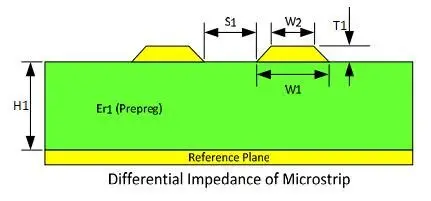
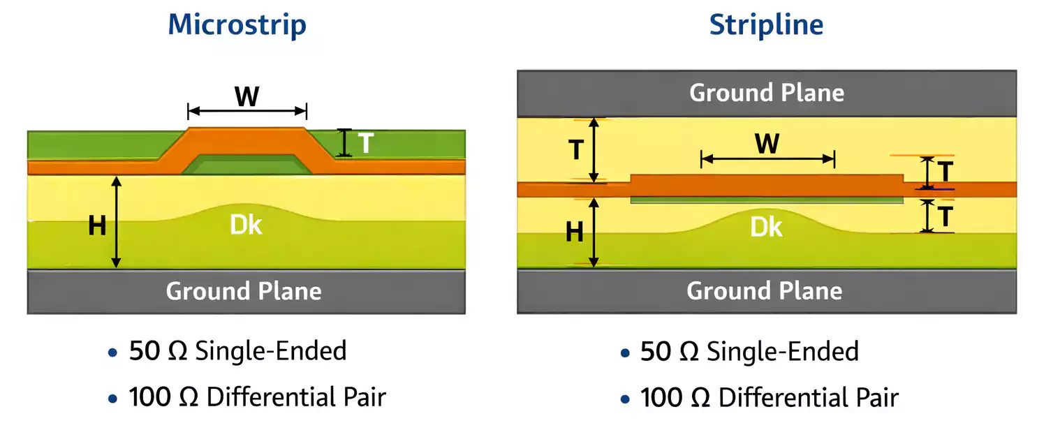
In PCB design, aspect ratio refers to the geometric proportion between the trace width and the dielectric thickness separating the signal trace from its reference plane. For microstrip lines, this is the distance from the top copper trace to the ground plane below, while in striplines, it involves the spacing between two ground planes. A higher aspect ratio, meaning a wider trace relative to the dielectric height, reduces characteristic impedance by increasing capacitance. Conversely, a lower aspect ratio elevates impedance due to decreased capacitive coupling. This parameter is fundamental to PCB aspect ratio impedance control strategies. Industry guidelines, such as those in IPC-2141A, emphasize balancing these dimensions to achieve target impedances like 50 ohms single-ended or 100 ohms differential.
The relevance of aspect ratio intensifies in high-frequency PCB environments, where wavelength approaches trace lengths, turning them into transmission lines. Without controlled impedance, mismatches cause standing waves, voltage peaks, and power loss. Dielectric thickness variations during lamination can alter the effective aspect ratio, amplifying these effects. Engineers target specific ratios based on stackup requirements, ensuring traces maintain uniform impedance across the board. This control preserves signal integrity by minimizing return loss and insertion loss. For electric engineers, mastering aspect ratio calculations streamlines design iterations and reduces fabrication yields issues.
Technical Principles of Aspect Ratio and Impedance
Characteristic impedance in PCB traces derives from transmission line theory, where Z0 equals the square root of inductance per unit length over capacitance per unit length. Trace width primarily affects inductance, while dielectric thickness governs capacitance through the electric field distribution. Increasing dielectric thickness decreases capacitance, raising Z0 for a fixed trace width, thus lowering the aspect ratio. In microstrip configurations, the air above the trace modifies the effective dielectric constant, making aspect ratio adjustments more sensitive to material properties. Striplines, fully embedded, offer more predictable behavior but require symmetric dielectric thicknesses around the trace.
Fabrication tolerances on dielectric thickness, often 10 percent or more, necessitate compensatory trace width adjustments to hold impedance within 5 to 10 percent. Aspect ratio optimization involves iterative modeling of fields using conformal mapping or finite element methods outlined in standards like IPC-2221. Copper roughness and skin effect further complicate high-frequency behavior, where effective dielectric thickness influences loss tangent. Engineers simulate these interactions to predict impedance profiles. Maintaining a consistent aspect ratio across layers prevents intra-layer discontinuities. This structured approach ensures high-frequency PCB traces behave as ideal transmission lines.
Dielectric materials with low dissipation factors are paired with precise aspect ratios to minimize attenuation. Variations in glass weave within the prepreg can create local impedance fluctuations if aspect ratio is not accounted for. Reference planes must be continuous to stabilize the return path, amplifying the aspect ratio's role. At frequencies above 10 GHz, radiation losses in microstrips demand higher aspect ratios for confinement. These principles guide electric engineers in stackup definition.
Key Factors Affecting Aspect Ratio in Impedance Control
Trace width directly scales with aspect ratio to target Z0; wider traces lower impedance by enhancing coupling. Dielectric thickness, controlled during pressing, sets the baseline for this ratio, with thinner cores enabling finer features but risking shorts. Material dielectric constant interacts multiplicatively, requiring aspect ratio recalibration for different resins. Copper weight influences trace thickness, subtly shifting effective width. Vias introduce discontinuities, where stub lengths alter local aspect ratio equivalents.
Fabrication processes like sequential lamination impact final dielectric heights, demanding margin in initial designs. Etch tolerances on trace width, typically 10 to 20 percent, couple with thickness variations to challenge control. High-frequency PCB demands often specify impedance test coupons at board edges for verification. Aspect ratio mismatches between layers cause mode conversion in differential pairs. Engineers address these through symmetric stackups.
Best Practices for Maintaining Signal Integrity
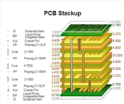
Start with stackup planning, defining dielectric thicknesses to support required trace widths for target impedances. Use symmetric builds to equalize aspect ratios across signal layers, per IPC-6012E qualification specs. Specify impedance tolerances early, typically plus or minus 10 percent, and include TDR test structures. Collaborate on material selection for consistent Er and low loss. Simulate aspect ratio sensitivities to process variations before layout.
During routing, maintain uniform trace lengths and avoid sharp bends that alter effective width. For differential pairs, match aspect ratios between traces for balanced impedance. Post-etch inspection verifies widths, with adjustments in artwork for etch factor. High-frequency PCB verification involves VNA sweeps on coupons to confirm Z0. Layer sequencing prioritizes signal layers near planes for optimal aspect ratios. These practices ensure robust signal integrity.
Incorporate ground stitching vias to reinforce reference planes, stabilizing fields. Monitor panel warpage, as it compresses dielectrics unevenly, skewing thicknesses. Final fab drawings detail aspect ratio targets explicitly.
Troubleshooting Common Aspect Ratio Issues
Deviations often stem from dielectric thickness creep during lamination, raising Z0 unexpectedly. Measure as-built stackups via cross-sectioning to correlate with simulations. If traces etch narrower, increasing aspect ratio inversely, compensate by widening design widths. Crosstalk spikes indicate plane gaps disrupting fields; add more vias. High return loss points to via stubs; back-drill or use blind vias.
For high-frequency PCB, eye diagram closure flags cumulative effects. Adjust via aspect ratios in HDI to avoid capacitance bumps. Iterative fab reviews refine models. These diagnostics preserve signal integrity.
Conclusion
PCB aspect ratio impedance control is essential for high-frequency applications, directly tying trace width and dielectric thickness to signal integrity. By understanding transmission line fundamentals and applying structured design practices, engineers achieve precise Z0 control. Standards like IPC-2141A and IPC-6012E provide frameworks for reliability. Proactive stackup optimization and verification minimize risks. Ultimately, mastering aspect ratio ensures high-performance PCBs that meet demanding electrical requirements.
FAQs
Q1: What role does PCB aspect ratio play in controlled impedance traces?
A1: The PCB aspect ratio, defined as trace width divided by dielectric thickness, determines characteristic impedance in microstrip and stripline configurations. A higher ratio lowers Z0 by boosting capacitance, crucial for matching source and load in high-frequency PCB designs. Engineers adjust it to hit targets like 50 ohms, preventing reflections and maintaining signal integrity. Fabrication tolerances require modeling this ratio early.
Q2: How does dielectric thickness affect trace width in impedance control?
A2: Dielectric thickness inversely impacts impedance; thicker layers raise Z0, necessitating wider trace widths to restore the aspect ratio and lower it back to spec. In high-frequency PCB, precise control avoids signal distortion. Stackup symmetry ensures consistent thicknesses. Verification via coupons confirms compliance.
Q3: Why is signal integrity critical in high-frequency PCB with aspect ratio variations?
A3: Aspect ratio inconsistencies cause impedance mismatches, leading to reflections, jitter, and data errors in high-speed links. Controlled impedance traces via optimized ratios preserve waveform fidelity. Best practices include symmetric designs and testing. This upholds performance in demanding applications.
Q4: What are best practices for PCB aspect ratio impedance control during design?
A4: Define stackups with targeted dielectric thicknesses, simulate aspect ratios for tolerances, and route uniform traces. Include impedance coupons for fab verification. Reference IPC guidelines for parameters. These steps ensure reliable signal integrity in controlled impedance traces.
References
IPC-2141A — Design Guide for High-Speed Controlled Impedance Circuit Boards. IPC
IPC-2221 — Generic Standard on Printed Board Design. IPC
IPC-6012E — Qualification and Performance Specification for Rigid Printed Boards. IPC


