 ALLPCB


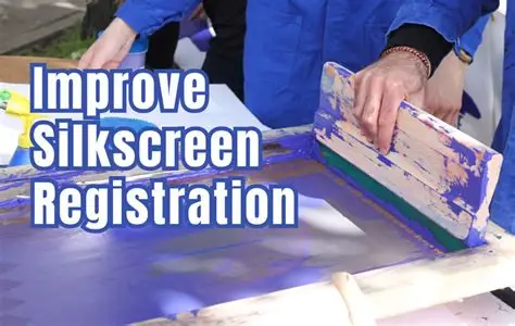
Introduction
Silkscreen misalignment occurs when the printed legend on a printed circuit board shifts from its intended position relative to the copper traces and pads. This offset can lead to significant expenses through increased scrap PCB boards and extended PCB production delays. Engineers often encounter these issues during high-volume manufacturing runs where even minor registration errors compound across thousands of units. Proper attention to silkscreen accuracy importance helps maintain assembly line efficiency and reduces the need for rework. Design for manufacturability practices that incorporate clear DFM silkscreen guidelines minimize these risks from the outset. Understanding the mechanisms behind misalignment allows teams to implement preventive measures that protect both schedule and budget.
Why Silkscreen Alignment Matters in PCB Production
Accurate silkscreen placement supports reliable component identification and orientation during assembly. When misalignment exceeds acceptable tolerances, operators may place parts incorrectly, resulting in functional failures that only appear after testing. Such defects drive up the overall silkscreen misalignment cost by forcing entire batches into quarantine or scrap. Procurement teams notice the downstream effects through longer lead times and higher unit pricing on replacement orders. Industry standards such as IPC-A-600 establish visual and dimensional criteria that define acceptable limits for legend registration. Meeting these criteria consistently improves yield rates and supports predictable manufacturing timelines.
Technical Principles and Mechanisms of Misalignment
Silkscreen printing relies on precise alignment between the stencil or screen and the underlying substrate. Thermal expansion of the board material during curing cycles can shift the reference points used for registration. Mechanical stress from handling or fixturing may also introduce small offsets that accumulate across multiple process steps. In multilayer constructions, cumulative tolerances from inner layer imaging and outer layer printing further increase the chance of legend drift. Engineers evaluate these factors through stack-up analysis and material property data to predict potential movement. When offsets exceed the thresholds outlined in IPC-6012, boards fail visual inspection and enter the scrap stream.
Related Reading: Precision PCB Silkscreen Alignment: Achieving Perfect Registration for Error-Free Assembly
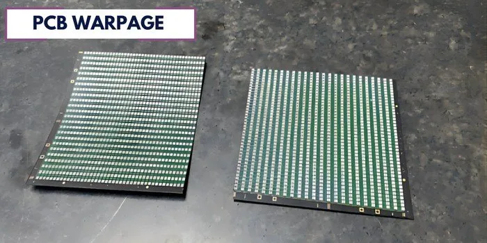
Causes of Offset in Manufacturing Environments
Several process variables contribute to silkscreen misalignment. Screen tension variations or improper emulsion thickness can cause the legend to stretch or compress during printing. Substrate warpage induced by moisture absorption or uneven heating creates a moving target for the printer. Tooling pin wear or fixture misalignment compounds these effects, especially on large panels processed at high speed. Environmental controls such as temperature and humidity stability in the print room play a direct role in maintaining registration accuracy. Monitoring these parameters through statistical process control helps identify drift before it produces unacceptable results.
Related Reading: Troubleshooting Silkscreen Alignment Issues in PCB Manufacturing: A Practical Guide
Practical Solutions and DFM Silkscreen Guidelines
Design teams reduce misalignment risk by specifying adequate clearance between legend elements and copper features. Placing fiducial marks or alignment targets in the artwork allows automated optical inspection systems to verify registration after printing. Selecting solder mask and silkscreen inks with matched thermal expansion characteristics limits differential movement during curing. Manufacturers apply DFM silkscreen guidelines that define minimum line widths, character heights, and registration tolerances tailored to the chosen process. Early collaboration between design and production engineers catches potential issues before artwork release. Regular calibration of printing equipment and verification of fixture condition further stabilize output quality.
Best Practices for Inspection and Process Control
Incoming material inspection includes checks for panel flatness and dimensional stability. After silkscreen application, automated vision systems compare printed legend positions against the copper pattern using reference points defined in the design files. Any deviation beyond established limits triggers immediate process adjustment or board rejection. Documentation of registration data across multiple lots reveals trends that point to equipment or material issues. Implementing these controls consistently lowers the incidence of scrap PCB boards and shortens overall cycle times.
Conclusion
Offset silkscreen creates measurable financial impact through scrap, delays, and lost productivity. Structured attention to material behavior, process parameters, and design rules prevents most registration errors. Adherence to recognized standards such as IPC-A-600 and IPC-6012 provides objective benchmarks that guide both design and manufacturing decisions. Teams that integrate these practices achieve higher first-pass yields and more reliable delivery performance.
FAQs
Q1: What factors contribute most to silkscreen misalignment cost in high-volume PCB runs?
A1: Material expansion, fixture wear, and print parameter drift are primary drivers. These issues lead to rejected panels that increase scrap PCB boards and extend production schedules. Early application of DFM silkscreen guidelines during layout reduces the frequency of such defects.
Q2: How does silkscreen accuracy importance affect PCB production delays?
A2: Misaligned legend forces additional inspection steps and potential rework loops. Boards that fail registration checks move to quarantine, interrupting the normal flow through assembly and test. Consistent process monitoring keeps throughput stable and protects committed delivery dates.
Q3: Which DFM silkscreen guidelines help prevent offset during manufacturing?
A3: Clearance rules between legend and copper, specified fiducial placement, and defined registration tolerances form the core of effective guidelines. These specifications allow printers to maintain alignment within limits established by industry standards. Following them from the design stage minimizes downstream corrections.
Q4: Can improved inspection reduce scrap PCB boards caused by silkscreen issues?
A4: Automated optical systems that verify legend position against copper features catch offsets before boards proceed to assembly. Statistical tracking of registration data highlights process trends that require correction. This approach lowers rejection rates and supports higher overall yield.


