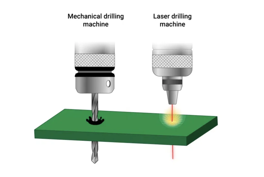
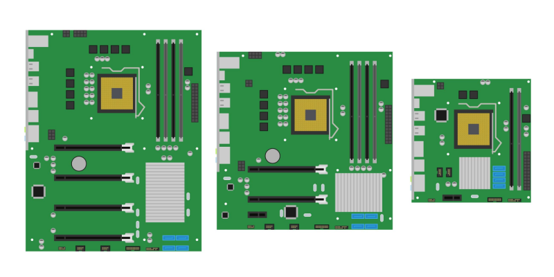
In the world of PCB production, panel size optimization is a critical factor in achieving both efficiency and precision. How do you balance the need for high-volume output with the demand for defect-free, high-quality boards? The answer lies in strategic panel design. By carefully selecting panel sizes and layouts, manufacturers can boost PCB production efficiency, improve yield, and minimize defects. In this blog, we’ll dive deep into the art of panel size optimization, exploring key considerations for precision PCB manufacturing and high-volume production.
Why Panel Size Matters in PCB Production Efficiency
Panel size plays a pivotal role in streamlining the manufacturing process. When multiple PCBs are arranged on a single panel, it reduces material waste, speeds up assembly, and lowers costs. However, choosing the right panel size isn’t just about fitting as many boards as possible. It’s about finding a balance that maximizes efficiency without compromising quality.
In high-volume production, larger panels often mean fewer handling steps and faster processing through automated equipment like stencil printers and reflow ovens. For instance, using standard laminate sizes such as 18 x 24 inches can increase board yield by up to 20%, translating to significant cost savings. However, oversized panels can lead to issues like warping or uneven heat distribution during soldering, which may cause defects. This is where panel size optimization becomes an art form—balancing output with precision.
Key Factors in Panel Size Optimization for Precision PCB Manufacturing
Optimizing panel size requires a deep understanding of several factors that influence both efficiency and quality. Below, we break down the most important considerations for achieving precision in PCB manufacturing.
1. Material Utilization and Waste Reduction
One of the primary goals of panel size optimization is to make the most of raw materials. Standard panel sizes, such as 21 x 24 inches, are often used to minimize scrap. By arranging PCBs in a tight, efficient layout, manufacturers can reduce waste and lower production costs. For example, a well-designed panel layout can save up to 30% in material costs compared to poorly planned designs.
However, cramming too many boards into a panel can lead to insufficient spacing, increasing the risk of damage during depanelization. A smart strategy is to use software tools to simulate layouts and identify the most material-efficient arrangement without sacrificing quality.
2. Compatibility with Automated Equipment
Modern PCB production relies heavily on automation for speed and accuracy. Panels must be sized to fit seamlessly into automated assembly lines. If a panel is too large or too small for the equipment, it can cause misalignment, delays, or even damage to the boards. Ensuring that panel dimensions align with the specifications of pick-and-place machines and reflow ovens is essential for maintaining precision in high-volume production.
For instance, panels that are too narrow may not provide enough stability during processing, leading to vibration or misalignment. On the other hand, overly large panels might not fit within the equipment’s working area, forcing manual handling that introduces human error.
3. Thermal and Mechanical Stability
During processes like reflow soldering, panels are exposed to high temperatures that can cause warping or uneven heat distribution. Larger panels are more prone to thermal stress, which can lead to defects like solder joint failures or impedance mismatches. For critical applications where controlled impedance is vital—say, maintaining a 50-ohm impedance for high-speed signals—thermal stability is non-negotiable.
To address this, manufacturers often add process edges or rails to panels. These extra borders provide structural support and help distribute heat evenly. A typical process edge might be 0.5 inches wide, adding stability without wasting too much material. Balancing panel size with thermal and mechanical considerations ensures precision in the final product.
High-Volume Panel Considerations: Maximizing Yield and Minimizing Defects
In high-volume PCB production, the stakes are higher. Every small inefficiency or defect can multiply across thousands of boards, leading to significant losses. Here, panel size and yield are closely linked, and a well-thought-out panel strategy is key to success.
1. Panel Size and Yield: Finding the Sweet Spot
Yield refers to the percentage of usable boards produced from a panel. A higher yield means less waste and lower costs. Optimizing panel size directly impacts yield by determining how many boards can be fabricated in one go. For example, a panel layout that fits 50 small boards with minimal spacing can achieve a yield of over 90%, while a poorly designed layout might drop to 70% or lower due to wasted space or damaged boards.
However, larger panels aren’t always better for yield. If a panel is too big, it may require more complex depanelization techniques, increasing the risk of cracks or stress damage. Techniques like V-scoring or tab-routing can help, but they must be planned carefully during the design phase to avoid defects.
2. Minimizing Defects with a Smart Panel Strategy
Defects are the enemy of high-volume production. A single flaw, such as a misaligned component or a cracked board, can render an entire batch unusable. Panel size optimization plays a crucial role in minimizing defects by ensuring consistent processing conditions across all boards on the panel.
For instance, uniform spacing between boards reduces the risk of uneven soldering. Leaving a gap of at least 0.1 inches between boards allows for proper heat distribution and prevents solder bridges. Additionally, adding fiducial marks—small reference points on the panel—helps automated equipment align components with precision, reducing placement errors by up to 15% in some studies.
Strategies for Effective Panel Size Optimization
Now that we’ve covered the key factors and challenges, let’s explore actionable strategies for optimizing panel size in PCB production. These tips will help manufacturers achieve both efficiency and precision, even in high-volume scenarios.
1. Use Software for Panel Layout Simulation
Advanced design software can simulate different panel layouts to find the most efficient arrangement. These tools analyze factors like material usage, spacing, and compatibility with manufacturing equipment. By testing multiple configurations virtually, manufacturers can avoid costly trial-and-error on the production floor.
For example, software might recommend a layout that fits 40 boards on a 18 x 24-inch panel with only 5% material waste. This data-driven approach ensures that panel size optimization is based on real numbers, not guesswork.
2. Incorporate Process Edges and Breakaway Tabs
Adding process edges or breakaway tabs to panels provides extra support during manufacturing. These features prevent boards from shifting or breaking during handling and depanelization. A common practice is to add a 0.25-inch edge around the panel, which can be easily removed after assembly without damaging the boards.
This strategy is especially useful for smaller boards that are more prone to damage. It enhances structural stability and reduces defect rates, particularly in high-volume runs.
3. Test Panel Designs in Small Batches
Before committing to full-scale production, test your panel design with a small batch. This allows you to identify potential issues like warping, misalignment, or thermal stress without risking an entire run. For instance, a test batch might reveal that a panel size of 21 x 24 inches causes uneven soldering due to heat distribution issues, prompting a switch to a smaller size like 18 x 24 inches.
Small-batch testing is a cost-effective way to refine your panel strategy and ensure precision in the final product.
Challenges in Balancing Efficiency and Precision
While panel size optimization offers clear benefits, it’s not without challenges. One common issue is the trade-off between efficiency and quality. Larger panels may speed up production but can introduce risks like thermal stress or handling damage. Conversely, smaller panels might ensure precision but slow down output and increase costs.
Another challenge is adapting to diverse board designs. A panel layout that works perfectly for one type of PCB might be inefficient for another due to differences in size, shape, or component density. Manufacturers must remain flexible and willing to adjust their panel strategy for each project.
The Future of Panel Size Optimization in PCB Production
As technology advances, so do the tools and techniques for panel size optimization. Emerging trends like AI-driven design software and fully automated production lines are making it easier to achieve both efficiency and precision. For example, AI algorithms can predict the optimal panel size for a given board design by analyzing factors like material costs, yield rates, and defect risks.
Additionally, innovations in materials—such as more heat-resistant laminates—allow for larger panels without the risk of thermal damage. These advancements promise to push the boundaries of high-volume PCB production, making it faster, cheaper, and more reliable.
Conclusion: Mastering the Art of Panel Size for PCB Success
Panel size optimization is both a science and an art in PCB production. By carefully balancing efficiency and precision, manufacturers can achieve higher yields, lower costs, and fewer defects. Whether you’re focusing on material utilization, equipment compatibility, or thermal stability, a smart panel strategy is the key to success in precision PCB manufacturing and high-volume production.
From using software for layout simulation to testing designs in small batches, the strategies outlined in this blog provide a roadmap for optimizing panel size. As the industry continues to evolve, staying ahead of the curve with innovative tools and techniques will ensure that your PCB production process remains efficient and defect-free.
By mastering the art of panel size, you can transform challenges into opportunities, delivering high-quality boards that meet the demands of today’s fast-paced electronics market.
 ALLPCB


