If you're struggling with PCB warpage and looking for a practical solution, V-scoring could be the answer. This technique helps manage stress in printed circuit boards (PCBs) during manufacturing and assembly, reducing the risk of bending or deformation. In this guide, we'll dive deep into how V-scoring works, why it’s effective against warpage, and how it ties into surface mount technology (SMT) processes. By the end, you'll have actionable steps to implement V-scoring in your designs and improve PCB reliability.
What Is PCB Warpage and Why Does It Matter?
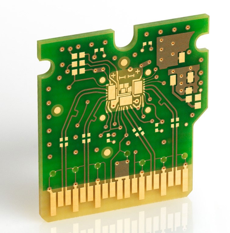
PCB warpage refers to the unintended bending or twisting of a circuit board during manufacturing, assembly, or operation. This deformation can lead to serious issues like poor solder joint formation, component misalignment, and even complete board failure. Warpage often occurs due to uneven thermal expansion, imbalanced copper distribution, or mechanical stress during processes like reflow soldering in SMT.
The impact of warpage is significant. For instance, a warped board can cause inconsistent solder paste application, leading to defects in up to 30% of SMT assemblies if not addressed. It also complicates automated assembly processes, increasing production costs and time. Understanding and mitigating warpage is crucial for ensuring high-quality, reliable electronics.
Understanding the Role of V-Scoring in PCB Design
V-scoring is a fabrication technique used to create V-shaped grooves on the top and bottom surfaces of a PCB. These grooves, typically cut to about one-third of the board's thickness, act as predetermined breaking points for separating individual boards from a larger panel after assembly. This method is widely used because it’s cost-effective and scalable for high-volume production.
Beyond simplifying depanelization, V-scoring plays a vital role in managing mechanical stress. By strategically placing these grooves, designers can control how stress distributes across the board during thermal cycles or handling. This stress relief is a key factor in minimizing warpage, especially for thinner boards or those with complex layouts.
How V-Scoring Helps Prevent PCB Warpage
V-scoring reduces warpage by addressing mechanical stress at its source. During manufacturing, PCBs are often subjected to high temperatures, especially in SMT reflow ovens where temperatures can reach 250°C. Uneven heating or cooling can cause the board to bend if stress isn’t managed properly. V-scoring creates controlled weak points that allow the board to flex slightly without deforming permanently.
Additionally, V-scoring helps maintain structural integrity during panel handling. Large panels are more prone to bending under their own weight or during automated pick-and-place operations. By incorporating V-scores, the panel remains rigid enough for processing but can be separated without inducing stress that leads to warpage in individual boards.
For example, a study of PCB manufacturing processes showed that panels with V-scoring had a 20% lower incidence of warpage compared to those using alternative separation methods like manual breaking or shearing. This demonstrates how a simple design choice can significantly improve outcomes.
Key Design Considerations for V-Scoring to Combat Warpage
Implementing V-scoring effectively requires careful planning. Here are some practical tips to ensure it helps reduce warpage in your PCBs:
1. Placement of V-Scores
Place V-scores along straight lines where stress concentration is minimal. Avoid placing them near high-density component areas or critical traces, as this can weaken the board unnecessarily. Keep a clearance of at least 0.3 mm from components to prevent damage during separation.
2. Panel Layout Optimization
Design your panel layout to balance copper distribution across layers. Uneven copper can cause thermal imbalance, exacerbating warpage. Use V-scoring to divide the panel into symmetrical sections, reducing stress points. For instance, a 4x4 array of small boards often warps less than an irregular layout when V-scored properly.
3. Material and Thickness Selection
Choose board materials with lower coefficients of thermal expansion (CTE), such as FR-4 with a CTE of around 14-17 ppm/°C. Thinner boards (under 1.6 mm) are more susceptible to warpage, so V-scoring becomes even more critical for these designs. Ensure the scoring depth is proportional to the board thickness—typically one-third—to avoid excessive weakening.
V-Scoring in Surface Mount Technology (SMT) Assembly
Surface Mount Technology (SMT) is a cornerstone of modern electronics manufacturing, allowing for compact, automated assembly of components directly onto the PCB surface. However, SMT processes, particularly reflow soldering, are a major contributor to PCB warpage due to high thermal stress. V-scoring integrates seamlessly into SMT workflows to mitigate these risks.
During SMT assembly, PCBs undergo multiple thermal cycles. For example, a typical reflow profile might involve preheating to 150°C, peaking at 245°C, and cooling back to room temperature. Without proper stress management, these cycles can cause warpage, leading to defects like tombstoning or open solder joints. V-scoring helps by providing controlled flexibility, ensuring the board remains flat during these temperature changes.
Moreover, V-scoring supports SMT by enabling efficient panelization. Assembling multiple boards in a single panel reduces handling time and improves throughput. Once assembly is complete, V-scored panels can be separated with minimal mechanical stress, preserving the integrity of delicate SMT components.
Best Practices for Combining V-Scoring and SMT
To maximize the benefits of V-scoring in SMT assembly, consider these best practices:
- Thermal Management: Use thermal profiling to ensure even heating across the panel. Place V-scores in areas less exposed to thermal gradients, as uneven heating can still cause localized warpage.
- Component Keep-Out Zones: Maintain a keep-out zone of at least 5 mm from V-score lines for SMT components. This prevents damage during depanelization and reduces stress on solder joints near the scoring area.
- Panel Support: During reflow, use proper fixtures or carriers to support the panel and prevent sagging. V-scoring works best when the panel is held flat during high-temperature processes.
Common Challenges with V-Scoring and How to Overcome Them
While V-scoring is a powerful tool against PCB warpage, it’s not without challenges. Here’s how to address some common issues:
1. Over-Scoring or Under-Scoring
If the V-groove is too deep, the panel may break prematurely during assembly. If too shallow, separation becomes difficult and can induce stress. Stick to a standard depth of one-third the board thickness (e.g., 0.5 mm for a 1.6 mm board) and verify with your manufacturer.
2. Misalignment of Scores
Misaligned V-scores can create uneven stress distribution, worsening warpage. Use precise CAD tools to define scoring lines and confirm alignment during fabrication setup. Double-check tolerances, aiming for a scoring accuracy of ±0.1 mm.
3. Component Damage During Separation
Depanelizing along V-scores can stress nearby components, especially in SMT designs with small, delicate parts. Use a manual or low-stress depaneling tool to minimize vibration, and ensure keep-out zones are respected in the design phase.
Advanced Tips for Reducing Warpage Beyond V-Scoring
While V-scoring is effective, combining it with other strategies can further reduce PCB warpage:
- Balanced Layer Stackup: Design your PCB with symmetrical copper layers to minimize thermal imbalance. For a 4-layer board, ensure copper weights (e.g., 1 oz/ft2) are consistent across layers.
- Pre-Baking: Pre-bake PCBs at 120°C for 2-4 hours before assembly to remove moisture, which can cause uneven expansion and warpage during reflow.
- Edge Rails: Add edge rails (extra material around the panel) during design to provide additional support. These can be combined with V-scoring for easier removal post-assembly.
Why V-Scoring Is a Must for Modern PCB Manufacturing
In today’s fast-paced electronics industry, managing PCB warpage is non-negotiable for producing reliable, high-performance products. V-scoring stands out as a practical, cost-effective solution that not only simplifies depanelization but also plays a critical role in stress management. When integrated into SMT assembly processes, it ensures boards remain flat and functional, even under the most demanding conditions.
By following the design tips and best practices outlined in this guide, you can leverage V-scoring to significantly reduce warpage in your PCBs. From optimizing panel layouts to maintaining proper clearances, every detail matters. As manufacturing technologies evolve, combining V-scoring with other warpage prevention techniques will keep your designs ahead of the curve.
Conclusion: Take Control of PCB Warpage with V-Scoring
PCB warpage is a challenge that can derail even the best designs, but with V-scoring, you have a powerful tool to fight back. This technique offers a straightforward way to manage stress, improve panel handling, and ensure reliability in SMT assembly. Start by incorporating V-scoring into your next project, paying close attention to placement, depth, and thermal considerations. With these steps, you’ll be well on your way to flatter, more dependable PCBs.
For engineers and designers, mastering V-scoring is an investment in quality and efficiency. Apply the insights from this guide to enhance your manufacturing process and deliver electronics that stand the test of time.
 ALLPCB


