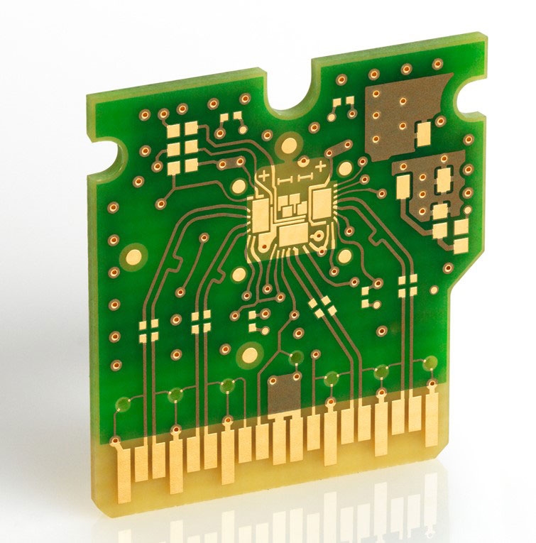
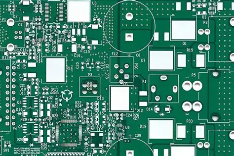
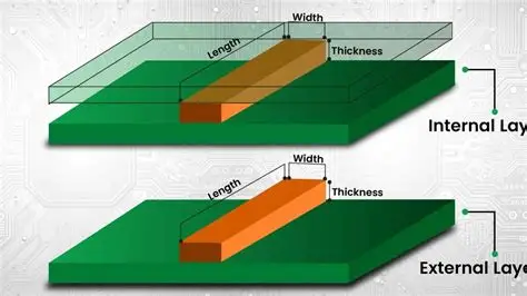
PCB thickness plays a significant role in trace-to-pad spacing considerations, directly affecting signal integrity, impedance control, and manufacturability. As a key factor in PCB thickness design, the board's thickness influences how closely traces and pads can be placed while maintaining performance and reliability. Thicker boards often allow for more layers and better heat dissipation but may complicate spacing due to increased dielectric distances. Conversely, thinner boards, common in High-Density Interconnect (HDI) designs, demand tighter spacing and precise manufacturing to avoid issues like crosstalk or signal loss.
In this comprehensive guide, we’ll explore how board thickness considerations impact trace-to-pad spacing, dive into the relationship with PCB stackup trace spacing, and provide practical insights for optimizing your designs. Whether you're working on standard or HDI boards, understanding these factors is crucial for creating reliable and efficient circuits.
Understanding PCB Thickness and Its Role in Design
PCB thickness refers to the overall height of the board, typically measured in millimeters or mils (1 mil = 0.001 inches). Standard thicknesses range from 0.8 mm to 1.6 mm (31 to 63 mils), though specialized designs, especially in HDI applications, can be as thin as 0.4 mm or less. The thickness is determined by the number of layers, the type of materials used (like FR-4 or high-frequency laminates), and the application requirements.
Thickness impacts several design aspects, including mechanical strength, thermal management, and electrical performance. For trace-to-pad spacing, it influences the dielectric layer thickness between conductive layers in a multi-layer PCB stackup trace spacing setup, which in turn affects impedance and signal integrity. A thicker board might provide more space for routing multiple layers, but it can also increase the distance signals must travel through vias, potentially introducing delays or losses.
Trace-to-Pad Spacing: Why It Matters
Trace-to-pad spacing refers to the distance between a conductive trace (the copper line carrying signals or power) and the pad (the connection point for components or vias). Proper spacing is critical to prevent electrical interference, such as crosstalk or short circuits, and to ensure manufacturability. Spacing requirements are often dictated by industry standards like IPC-2221, which provides guidelines based on voltage, current, and environmental factors.
Inadequate spacing can lead to signal integrity issues, especially in high-speed designs where electromagnetic interference (EMI) becomes a concern. For instance, in a design operating at 5 GHz, improper spacing might cause signal reflections or loss, degrading performance. On the other hand, overly conservative spacing can waste valuable board real estate, particularly in compact HDI layouts where space is at a premium.
How PCB Thickness Affects Trace-to-Pad Spacing
The relationship between PCB thickness design and trace-to-pad spacing is multi-faceted, impacting electrical, mechanical, and manufacturing considerations. Let’s break it down into key areas:
1. Dielectric Thickness and Impedance Control
In a multi-layer PCB, the thickness of the dielectric material between layers directly affects the impedance of traces. Impedance is a measure of opposition to alternating current and is critical for high-speed signals. For example, a common target impedance for high-speed digital signals is 50 ohms. If the dielectric is thicker due to increased overall board thickness, the trace width must often be adjusted to maintain the target impedance, which can influence how closely traces and pads can be placed.
Thinner boards, often used in HDI designs, have thinner dielectric layers, allowing for tighter trace-to-pad spacing. However, this requires precise control during manufacturing to avoid issues like signal coupling. A typical HDI board might have dielectric layers as thin as 0.1 mm (4 mils), compared to 0.2 mm or more in standard boards, enabling spacing as low as 3 mils in some cases.
2. Signal Integrity and Crosstalk
Signal integrity is paramount in modern electronics, especially for high-speed applications like 5G or data centers. PCB thickness influences the separation between layers in a PCB stackup trace spacing configuration, which affects crosstalk—the unwanted coupling of signals between adjacent traces or pads. Thicker boards can reduce crosstalk between layers due to greater separation but may increase it within the same layer if spacing isn’t adjusted accordingly.
For instance, in a 1.6 mm thick board with a 4-layer stackup, the distance between the top and inner layers might be 0.3 mm, providing a natural barrier against interference. However, in a 0.8 mm thick HDI board with 6 layers, the dielectric might be only 0.1 mm, requiring tighter trace-to-pad spacing control (e.g., 4-5 mils) to prevent crosstalk.
3. Manufacturing Constraints
Board thickness considerations also tie into manufacturing capabilities. Thicker boards are generally easier to handle during fabrication and assembly, allowing for slightly relaxed spacing rules. However, thinner boards, especially in HDI designs, demand advanced manufacturing techniques like laser drilling for microvias and finer etching for tight trace-to-pad spacing (often below 5 mils).
Manufacturers typically specify minimum spacing based on their process capabilities. For example, a standard process might support 6-mil spacing on a 1.6 mm board, while an advanced HDI process could achieve 3-mil spacing on a 0.6 mm board. Exceeding these limits due to improper thickness planning can lead to defects like copper bridging or insufficient insulation.
4. Thermal and Mechanical Stability
Thicker PCBs offer better thermal dissipation and mechanical strength, which can indirectly influence spacing decisions. In power electronics, where heat generation is high, a thicker board (e.g., 2.0 mm) might be chosen to handle thermal loads, allowing for wider traces and pads with larger spacing (e.g., 10 mils or more) to manage current density. Conversely, thinner boards in portable devices prioritize compactness, pushing designers to minimize trace-to-pad spacing despite potential thermal challenges.
Special Considerations for High-Density Interconnect (HDI) Designs
High-Density Interconnect (HDI) technology is increasingly popular for compact, high-performance electronics like smartphones and wearables. HDI boards are typically thinner (0.4-0.8 mm) and feature microvias, blind vias, and buried vias to achieve higher routing density. This directly impacts trace-to-pad spacing in several ways:
- Tighter Spacing Requirements: HDI designs often require trace-to-pad spacing as low as 2-3 mils to accommodate dense component placement. For comparison, standard designs might use 6-8 mils.
- Thinner Dielectrics: With dielectric layers often below 0.1 mm, impedance control becomes more sensitive to spacing variations, demanding precise design and manufacturing.
- Advanced Materials: HDI boards may use specialized laminates with lower dielectric constants (e.g., 3.5 compared to 4.5 for FR-4), allowing tighter spacing without sacrificing signal integrity.
In HDI PCB stackup trace spacing, designers must balance the need for compactness with signal performance. For example, a 6-layer HDI board for a 5G module might use 3-mil spacing on inner layers to route high-speed signals at 10 Gbps, while maintaining strict impedance tolerances of ±10%.
Practical Tips for Optimizing Trace-to-Pad Spacing with PCB Thickness
Designing a PCB with the right thickness and spacing requires careful planning. Here are actionable tips to help you navigate board thickness considerations and achieve optimal performance:
- Match Thickness to Application: Choose a board thickness based on your project’s needs. For high-speed or HDI designs, opt for thinner boards (0.6-0.8 mm) to enable tighter spacing. For power or industrial applications, thicker boards (1.6-2.0 mm) provide durability and thermal management.
- Use Design Software Tools: Leverage PCB design software with built-in impedance calculators to determine the ideal trace width and spacing for your stackup. This ensures signal integrity across different thicknesses.
- Consult Manufacturer Guidelines: Early in the design phase, review your manufacturer’s capabilities for minimum spacing and thickness tolerances. This prevents costly redesigns due to unfeasible specifications.
- Simulate Signal Performance: For high-speed designs, use simulation tools to model crosstalk and signal loss based on your PCB stackup trace spacing and thickness. Adjust spacing as needed to meet performance goals.
- Prioritize Layer Planning: In multi-layer boards, plan your stackup to separate high-speed traces from power or ground planes with adequate dielectric thickness, reducing interference.
Common Challenges and How to Avoid Them
Navigating PCB thickness design and trace-to-pad spacing can present challenges. Here are some common pitfalls and solutions:
- Challenge: Insufficient Spacing in Thin Boards
Solution: Use advanced manufacturing processes for HDI designs and double-check spacing against signal integrity simulations. Aim for at least 3-4 mils in dense areas unless specified otherwise by your manufacturer. - Challenge: Impedance Mismatch Due to Thickness Variations
Solution: Specify tight tolerances for dielectric thickness during fabrication (e.g., ±10%) and adjust trace widths accordingly during design. - Challenge: Thermal Issues in Thin Boards with Tight Spacing
Solution: Incorporate thermal vias or heat sinks near high-current areas, and consider slightly thicker boards if thermal loads are significant.
Conclusion: Balancing PCB Thickness and Trace-to-Pad Spacing for Success
PCB thickness is a critical factor in trace-to-pad spacing considerations, influencing everything from signal integrity to manufacturability. Whether you’re designing a standard board or a complex High-Density Interconnect (HDI) layout, understanding how board thickness considerations impact spacing is essential for creating reliable, high-performance circuits. By carefully planning your PCB thickness design and optimizing PCB stackup trace spacing, you can achieve the perfect balance of compactness, performance, and durability.
At ALLPCB, we’re committed to supporting your design journey with advanced manufacturing capabilities and expert guidance. Whether you’re tackling tight spacing in HDI boards or managing impedance in multi-layer stackups, our team is here to help you bring your vision to life with precision and quality.
 ALLPCB


