 ALLPCB


Introduction
Noise coupling poses a common challenge in PCB design, especially for electronic hobbyists experimenting with amplifiers, sensors, or digital circuits. It occurs when unwanted signals from one part of the board interfere with another, degrading performance and introducing errors. Understanding and applying minimization techniques can transform a noisy prototype into a reliable build. This article explores practical strategies focused on PCB traces and components, helping hobbyists achieve cleaner signals without advanced tools. By following structured approaches, you can enhance circuit stability in projects like audio mixers or microcontroller setups. Key principles draw from established guidelines to ensure consistent results.
What Is Noise Coupling and Why It Matters
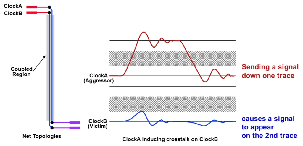
Noise coupling refers to the transfer of electrical noise between conductors on a PCB, primarily through capacitive or inductive mechanisms. Capacitive coupling happens via electric fields between nearby traces, while inductive coupling arises from magnetic fields generated by changing currents. In hobbyist projects, this manifests as crosstalk in audio lines or glitches in digital signals, leading to erratic behavior. For instance, a fast-switching digital trace can induce voltage spikes on an adjacent analog sensor line, skewing readings. Minimizing noise coupling is crucial for maintaining signal integrity, particularly in mixed-signal boards common among hobbyists. Reliable circuits mean fewer debugging hours and better project outcomes.
The relevance extends to real-world applications like home automation or drone controllers, where even minor noise can cause failures. Industry standards like IPC-2221 emphasize layout practices to control these effects, underscoring their importance in professional and amateur designs alike. Hobbyists benefit by adopting these early, avoiding costly respins.
Mechanisms and Causes of Noise Coupling
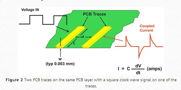
Noise coupling stems from electromagnetic interactions between PCB elements. When two traces run parallel and close, the electric field from one couples charge to the other, creating capacitive noise proportional to trace area and proximity. Inductive coupling increases with mutual inductance, especially in high-frequency signals where current loops enclose larger areas. Common-impedance coupling occurs through shared ground paths, where return currents superimpose noise on signals. Factors like trace length, width, and layer stacking amplify these effects in multi-layer boards.
Component placement exacerbates issues if high-speed parts neighbor sensitive ones, as switching transients radiate fields. Ground bounce from simultaneous switching further contributes via package inductance. Understanding these mechanisms allows targeted minimization techniques. For example, longer parallel runs heighten coupling, making routing strategy pivotal.
Environmental factors, such as board flexure or poor soldering, can indirectly worsen coupling by altering clearances. Adhering to design rules from IPC-2141 helps predict and mitigate these in controlled impedance layouts.
Minimization Techniques for PCB Traces
Effective minimization techniques start with optimizing PCB traces. Increase spacing between parallel traces to reduce capacitive coupling; wider gaps lower field overlap significantly. Route sensitive signals on inner layers surrounded by ground planes, which shield against external fields. Avoid right-angle bends that concentrate fields, opting for smooth curves or 45-degree turns instead. Stagger trace alignments across layers to break continuous coupling paths.
Guard traces, grounded on both sides of critical signals, absorb stray fields effectively. These act as barriers, shunting noise to ground before it reaches victims. In hobbyist tools, simulate simple stackups to verify. Combining these with via stitching along edges creates a Faraday cage-like effect for traces.
For high-speed hobby projects, control trace impedance through consistent width and dielectric thickness. Shorter traces inherently couple less, so minimize lengths while prioritizing signal flow. These techniques form the backbone of robust layouts.
Component Placement and Selection Strategies
Components play a key role in noise coupling minimization techniques. Position noise sources, like switching regulators, away from analog sections, using ground planes as barriers. Orient components to minimize loop areas; for example, place bypass capacitors close to power pins to shunt high-frequency noise locally. Decoupling capacitors across supplies filter common-mode noise before it couples via traces.
Shield sensitive components with grounded enclosures or copper pours connected to ground. Select parts with lower package inductance, such as QFN over DIP for high-speed signals. Proper orientation reduces parasitic coupling from leads. In mixed boards, group digital and analog components separately, with dedicated grounds.
Filtering components like ferrites or RC networks at interfaces block noise propagation. Hobbyists can prototype these on perfboards first to validate. Consistent application yields quieter boards.
Advanced Layout Best Practices
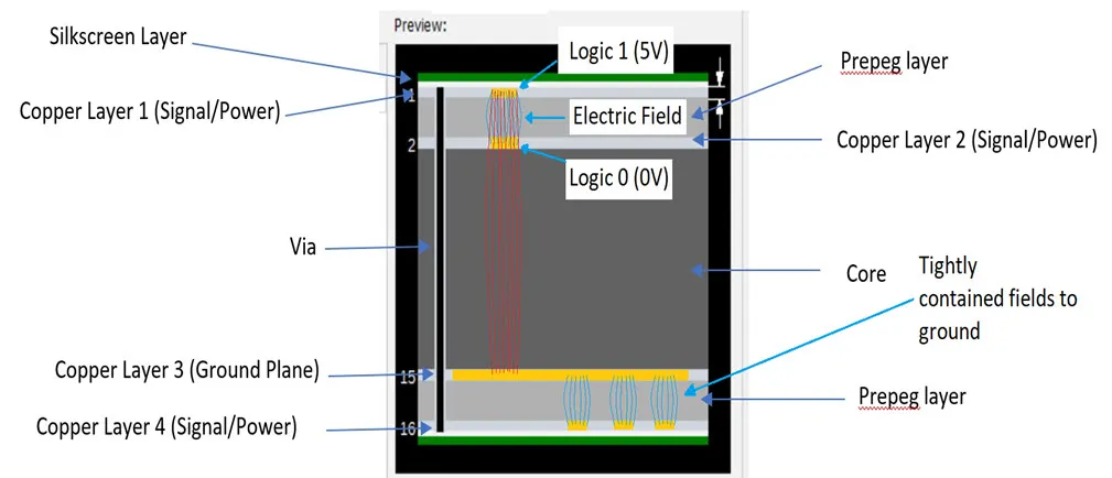
Implement solid ground planes on dedicated layers to provide low-impedance return paths, minimizing common-impedance coupling. Split planes only when necessary, stitching across splits with vias to prevent slot antennas. Power planes should overlay signals closely for tight coupling, reducing radiated noise. Layer stackup matters: signal-ground-signal sandwiches confine fields.
Via placement affects coupling; dense stitching around cutouts maintains shielding. Control board edge effects by keeping traces inset from edges. For hobbyists, four-layer boards offer a sweet spot for noise control without complexity.
Test iteratively with scopes to refine. These practices align with IPC-2221 guidelines for overall performance.
Troubleshooting Common Noise Coupling Issues
Spot noise coupling through symptoms like intermittent signals or frequency-dependent glitches. Use a scope to probe victim lines near aggressors, observing induced spikes. Isolate by lifting grounds or adding temporary shields. Check trace proximity against rules of thumb, like three times the trace width spacing.
Component-related issues often trace to poor decoupling; add ceramics and measure ripple. Simulate mentally: longer loops equal more inductance. Systematic checks reveal root causes quickly.
Conclusion
Mastering techniques to minimize noise coupling elevates PCB designs from functional to exceptional. Focus on trace spacing, ground planes, and strategic component placement for immediate gains. These minimization techniques, rooted in sound principles, suit electronic hobbyists tackling diverse projects. Consistent application reduces debugging and boosts reliability. Experiment iteratively, leveraging simple tools for validation. Cleaner boards await those who prioritize signal integrity from the start.
FAQs
Q1: What are the primary causes of noise coupling in PCB traces?
A1: Noise coupling in PCB traces arises mainly from capacitive fields between close parallels, inductive loops from currents, and shared ground impedances. Parallel runs over long distances amplify effects, especially at high frequencies. Hobbyists can mitigate by increasing spacing and using ground planes. Following IPC-2221 layout rules helps predict issues early.
Q2: How do ground planes aid in noise coupling minimization techniques?
A2: Ground planes provide low-impedance returns, shielding signals and absorbing stray fields to cut capacitive and inductive coupling. Place them adjacent to signal layers for best effect. Stitch edges with vias to maintain continuity. This simple addition transforms noisy hobby boards into stable ones.
Q3: What role do components play in reducing noise coupling?
A3: Components like decoupling capacitors near ICs shunt noise, preventing propagation through traces. Strategic placement separates noisy digital from quiet analog sections. Ferrite beads filter high frequencies effectively. Proper selection minimizes parasitic effects, enhancing overall minimization techniques.
Q4: Can hobbyists apply advanced minimization techniques on two-layer PCBs?
A4: Yes, on two-layer PCBs, route signals between ground pours and use wider spacing for traces. Add guard traces and keep loops small. Decoupling remains key for components. While multi-layers excel, disciplined routing yields good noise coupling control.
References
IPC-2221 — Generic Standard on Printed Board Design. IPC
IPC-2141 — Design Guide for High-Speed Controlled Impedance Circuit Boards. IPC


