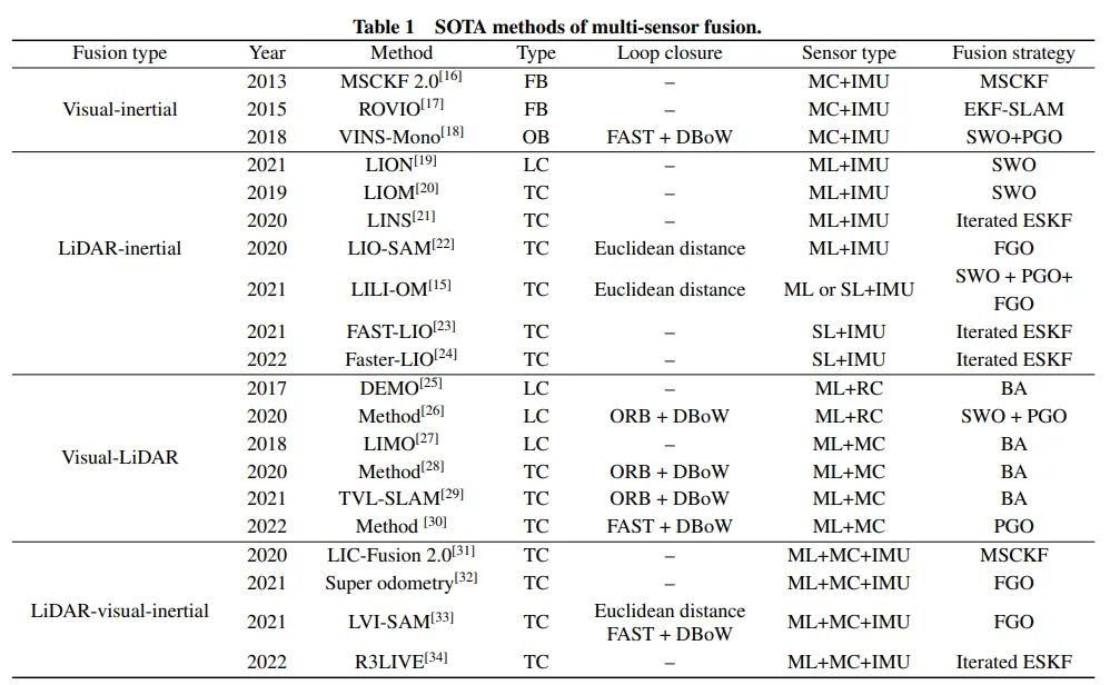
ALLPCB


Overview
CMOS image sensors (CIS) are widely used in products such as smartphones, digital cameras, and automotive cameras. They convert light into electrical signals and, with advances in CMOS process technology, have achieved high resolution, low noise, wide dynamic range, and on-chip intelligence. This article outlines the evolution of CMOS image sensors and compares stacked and single-chip (monolithic) CIS approaches, including their advantages, limitations, and typical applications.
History
The development of solid-state image sensors accelerated after the 1969 invention of the charge-coupled device (CCD) at Bell Labs. Research on CMOS image sensors began around the same time, but early CMOS devices suffered from poor image quality, low resolution, high noise, and limited light sensitivity, so CCDs dominated initially. Improvements in IC design and fabrication gradually eliminated these drawbacks, and CMOS sensors became the mainstream.
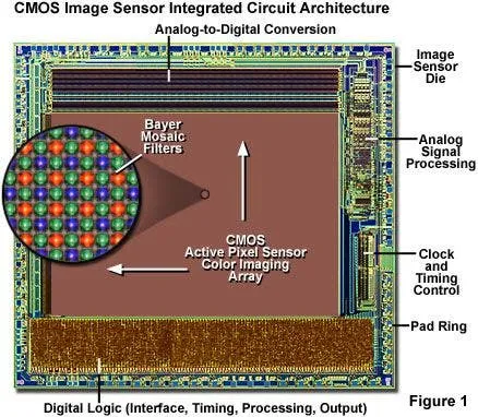
CMOS image sensors integrate photodiode arrays, analog readout, ADCs, digital logic, clock control, and I/O on a single chip. Photodiodes convert scene luminance and color into electrical signals, which are read out, converted to digital via ADCs, preprocessed, and transmitted via interfaces to host platforms.
There are multiple origin stories for the active-pixel CMOS sensor. One account credits Dr. Eric R. Fossum and colleagues at NASA's Jet Propulsion Laboratory for developing an active-pixel CMOS sensor in the 1990s and later commercializing it via Photobit. Another early contribution came from researchers at the University of Edinburgh in the late 1980s and 1990. Today, major CIS suppliers include Sony, Samsung, and Geke Micro.
CMOS Sensor Architectures
CMOS image sensors are commonly categorized by photodiode placement: front-side illumination (FSI), back-side illumination (BSI), and stacked (3D-stacked) structures based on BSI.
FSI sensors were common early on due to simpler processing, but with photodiodes located beneath metal and interconnect layers they receive less light, limiting performance. FSI designs are generally used for sensors below roughly 2 megapixels.
BSI flips the photodiode to the top, separating light collection from circuit layers. This reduces photon loss and increases quantum efficiency, improving low-light and outdoor performance, sensitivity, angular response, and reducing pixel crosstalk. The trade-off is increased process complexity and cost. BSI is typical for sensors above roughly 5 megapixels.
Stacked sensor architecture further separates the pixel layer and logic/circuit layers onto different wafers and then bonds them. In a stacked design, the top die retains only the photodiodes while all wiring, analog, and digital circuits are placed on the lower die. This increases the pixel-area fraction within the same chip footprint (from near 60% to nearly 90% in some implementations), reduces circuit noise, and enables smaller overall chip size for a given image quality, making stacked CIS the mainstream for high-megapixel applications.
Single-Chip High-Pixel Technology
An alternative to stacking is a monolithic single-chip high-pixel approach. Leveraging nearly two decades of process experience in single-wafer CMOS, some vendors have developed pixel and circuit process compatibility techniques that enable high-resolution imaging without stacking.
For example, Geke Micro developed a patented floating poly pixel isolation (FPPI) technique to support high pixel densities while controlling white spots and dark currents, maintaining image quality comparable to stacked products. Their GC32E1 sensor uses 0.7 μm pixels and demonstrates imaging performance similar to stacked equivalents.
The GC32E1 supports 32 MP full-pixel output and, combined with platform-level decoding (Remos aic), produces detailed, vivid photos. It also supports interleaved HDR for improved dynamic range in scenes with large brightness differences. Geke Micro has also optimized on-chip ADCs, digital circuits, and interface circuits so its single-chip high-pixel sensors can be compatible with module sizes designed for two-die stacked products, with only about a 10% area increase and a reduction in total silicon consumption of roughly 40%, improving wafer-area efficiency and cost structure.
Geke Micro products applying FPPI include models such as GC50B2, GC50E0, GC32E1, GC08A3, GC13A0, GC13A2, and GC16B3. A 32 MP single-chip CIS has been integrated into branded products and ramped to production, validating the feasibility and manufacturability of the single-chip route. The vendor plans to extend the platform to 50 MP and higher classes.
Conclusion
Stacked and single-chip CMOS image sensors are both important technical routes for high-resolution imaging. Stacked architectures currently dominate high-megapixel markets due to their area and noise advantages, while monolithic single-chip approaches are emerging as a viable alternative thanks to process and circuit innovations. As imaging applications in devices like smartphones mature and as related technologies such as AI and cloud computing evolve, CIS technology will continue to advance and diversify.