 ALLPCB


What Silkscreen Does and Why Alignment Matters
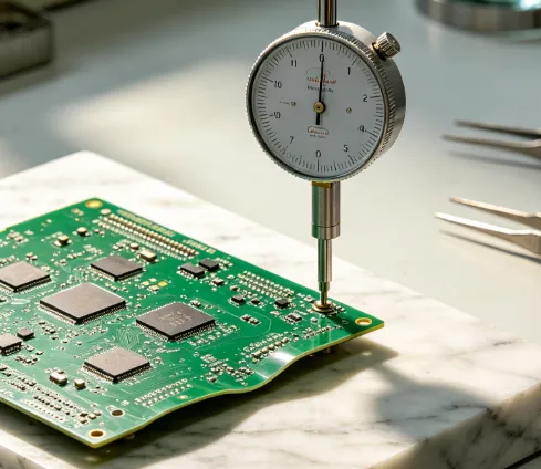
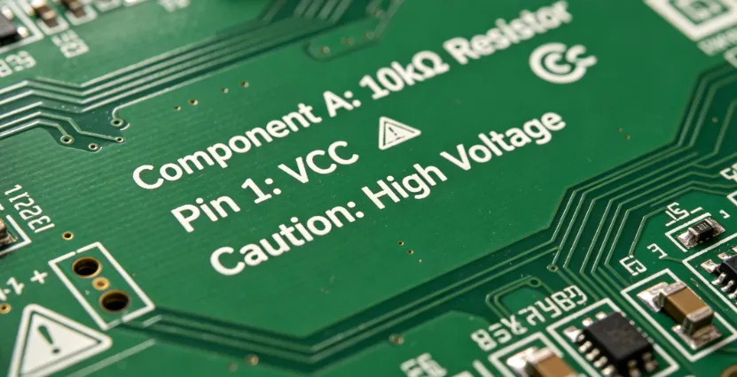
Silkscreen is the printed layer that carries text, symbols, and outlines on the surface of a PCB. It helps hobbyists identify part locations, orient components correctly, and follow assembly instructions without constant reference to schematic files. When the layer prints out of register, labels overlap pads or traces, making visual inspection difficult and increasing the chance of placement mistakes. Consistent alignment supports reliable hand soldering and rework, especially on boards with dense layouts or fine-pitch parts. For hobbyists working in small batches, even modest misalignment can turn an otherwise straightforward build into a prolonged troubleshooting session.
Common Causes of Silkscreen Misalignment
Several mechanical and process factors contribute to silkscreen offset during fabrication. Board warpage from uneven copper distribution or thermal stress can cause the substrate to shift slightly under the screen or laser imaging head. Inconsistent panel handling or fixture registration errors during printing also move the image relative to the copper layers. Hobbyists who order small prototype runs sometimes observe greater variation because the fabrication process has fewer automated checks than high-volume lines. Environmental factors such as humidity changes in the workshop can further affect film or stencil stability before imaging occurs. These mechanisms rarely produce dramatic defects, yet they accumulate into noticeable label drift that complicates later assembly steps.
Industry standards such as IPC-A-600K outline acceptable limits for registration accuracy and help hobbyists decide when a board requires correction rather than acceptance.
Related Reading: The High Cost of Offset Silkscreen: Preventing Misalignment in PCB Manufacturing
Practical Repair Techniques for Hobbyists
Silkscreen touch-up begins with a clean surface and good lighting. Hobbyists typically remove loose or overlapping ink with a fine abrasive pad or isopropyl alcohol wipe, taking care not to damage underlying copper. Once the area is prepared, a fine-tipped permanent marker or dedicated PCB ink pen can restore missing characters or lines by hand. For larger corrections, a small stencil cut from thin plastic or tape allows precise reapplication of symbols without bleeding onto adjacent features. After touch-up, a light coat of clear conformal coating or nail polish protects the new ink from abrasion during handling and soldering. These silkscreen repair techniques restore legibility quickly and keep projects moving without waiting for a new fabrication run.
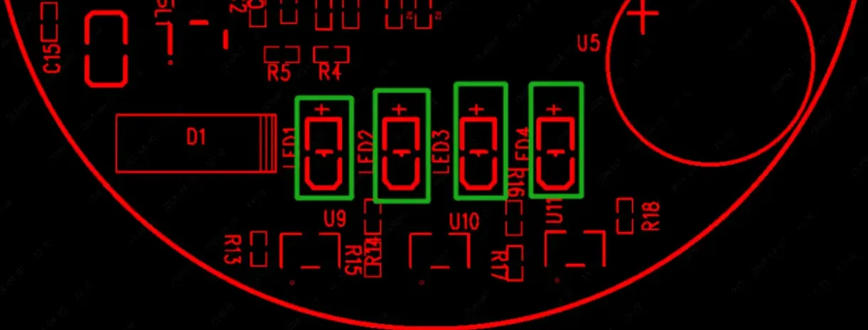
When misalignment affects critical areas such as pin-one indicators or test-point labels, silkscreen rework may involve selective removal followed by re-imaging on a spare board section if available. Hobbyists often photograph the original layout before correction so that restored markings match the intended positions exactly. Working under magnification reduces the risk of introducing new errors during manual application. Consistent technique across multiple boards builds familiarity and improves results over time.
Best Practices to Minimize Future Issues
Planning the silkscreen layer with slightly larger text and symbols gives fabrication tolerances more room before labels become unreadable. Hobbyists benefit from reviewing the design file at actual scale and confirming that all reference designators sit at least 0.5 mm away from copper features. Ordering a small test panel before committing to a full batch allows early detection of registration problems. Keeping boards flat during storage and avoiding extreme temperature swings in the workshop further reduces warpage-related shifts. These habits lower the frequency of silkscreen damage and reduce the need for repeated touch-up sessions.
Related Reading: PCB Silkscreen Design: Legibility and Industry Standards
Troubleshooting Workflow for Hobbyists
A systematic check starts with comparing the received board against the original design file using a printed paper overlay or digital measurement tool. Mark any offsets greater than the acceptable tolerance noted in IPC-6012E and decide whether touch-up or a new order is more practical. Next, test component placement on one or two boards to confirm that misaligned labels actually cause assembly errors. Document the locations and severity of each issue so that future orders can include clearer fabrication notes. This structured approach turns occasional silkscreen misalignment from a source of frustration into a manageable part of the hobbyist workflow.
Conclusion
Silkscreen misalignment arises from predictable mechanical and process variables that hobbyists can diagnose and correct with straightforward methods. Applying targeted repair techniques restores functionality while preserving the clarity needed for accurate assembly. Following simple design and handling practices reduces recurrence and keeps projects on schedule. With attention to registration and a few reliable touch-up skills, hobbyists maintain professional-looking boards even when small fabrication variations appear.
FAQs
Q1: How do I begin PCB silkscreen troubleshooting on a newly arrived board?
A1: Start by placing the board on a flat surface and comparing it directly to the design file using a ruler or digital calipers. Note any text or symbols that sit more than 0.3 mm away from their intended copper features. Clean the surface gently, then test-fit a few components to see whether the offset actually interferes with placement. This quick inspection identifies whether simple silkscreen touch-up will solve the problem or whether a new order is required.
Q2: What are the most effective silkscreen repair techniques for hobbyists?
A2: Fine abrasive cleaning followed by hand application with a permanent marker or ink pen works well for small corrections. For repeated symbols, a homemade stencil cut from thin plastic sheet provides consistent results without smearing. After restoration, a thin protective coating prevents the new ink from wearing during soldering. These steps return legibility quickly and avoid the cost of re-fabrication.
Q3: When should I consider silkscreen rework instead of touch-up?
A3: Silkscreen rework becomes worthwhile when multiple critical markings such as polarity indicators or connector labels are shifted enough to cause repeated placement errors. In such cases, hobbyists often prepare a replacement board section or order a small corrective panel. Documenting the exact offsets helps prevent the same issue on future orders.
Q4: How can I reduce the chance of silkscreen damage on future prototype orders?
A4: Review the silkscreen layer at 1:1 scale before submission and maintain at least 0.5 mm clearance from all copper. Request a small test panel first so any registration problems can be caught early. Store boards flat and away from heat sources to limit warpage that contributes to misalignment.
References
IPC-A-600K — Acceptability of Printed Boards. IPC, 2020
IPC-6012E — Qualification and Performance Specification for Rigid Printed Boards. IPC, 2017


