 ALLPCB


If you're diving into the world of printed circuit board (PCB) design, you’ve likely come across the term "silkscreen." But what exactly is the PCB silkscreen process, and why is it so important? In simple terms, silkscreen printing on a PCB is the process of adding text, symbols, and markings to the board's surface to identify components, test points, and other critical information. This layer, often applied using methods like screen printing, direct legend printing, or liquid photo imaging, plays a vital role in assembly, testing, and troubleshooting. In this comprehensive guide, we’ll explore the ins and outs of PCB silkscreen printing methods, breaking down each technique, its benefits, and key design considerations to help you master this essential step in PCB fabrication.
What Is PCB Silkscreen and Why Does It Matter?
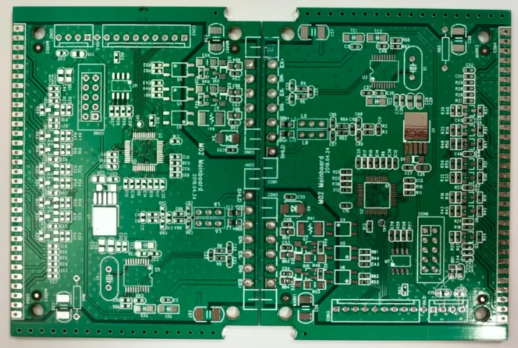
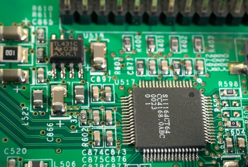
PCB silkscreen refers to the layer of ink applied to the surface of a printed circuit board. This layer includes labels, symbols, logos, and other markings that provide crucial information for engineers, technicians, and manufacturers. Typically placed on the component side of the board (though it can appear on the solder side in some cases), the silkscreen helps identify parts like resistors, capacitors, and connectors, as well as test points and warning symbols.
Without a clear silkscreen, assembling and servicing a PCB can become a nightmare. Imagine trying to place components on a densely populated board without labels or guides—it’s like solving a puzzle with no picture. The silkscreen ensures accuracy during assembly, simplifies troubleshooting, and even enhances the professional look of the final product by including branding or manufacturer details.
The Role of Silkscreen in PCB Design and Manufacturing
The silkscreen layer serves multiple purposes throughout the lifecycle of a PCB. During the design phase, it helps engineers communicate placement and orientation details. In manufacturing, it guides assembly teams to place components correctly. For testing and servicing, it allows technicians to quickly locate test points or identify specific parts without referring to schematics constantly.
Moreover, the silkscreen impacts the manufacturing process itself. A poorly designed silkscreen—such as overcrowded text or misplaced labels—can lead to errors during assembly or even affect the board’s performance if markings interfere with critical areas. That’s why understanding the PCB silkscreen process and choosing the right printing method is essential for a successful project.
Common PCB Silkscreen Printing Methods
There are three primary methods for applying silkscreen to a PCB: traditional screen printing, direct legend printing (DLP), and liquid photo imaging (LPI). Each method has its own advantages, limitations, and ideal use cases. Let’s dive into these PCB silkscreen printing methods to understand how they work and when to use them.
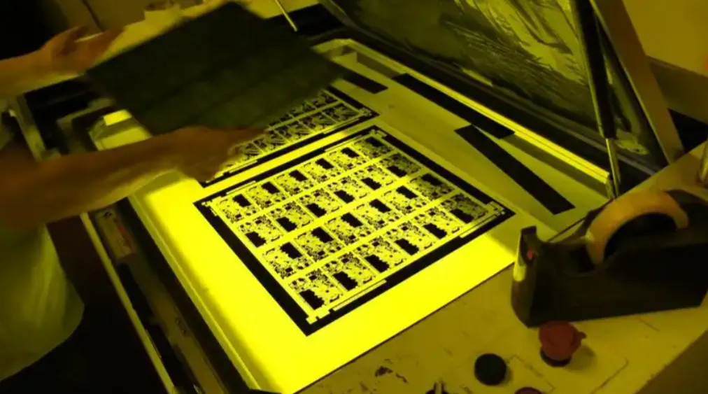
1. Traditional Screen Printing for PCB Silkscreen
Traditional screen printing is one of the oldest and most cost-effective methods for applying silkscreen to a PCB. In this process, a mesh screen (or stencil) with the desired design is placed over the PCB. Epoxy ink, which is non-conductive, is then pushed through the mesh onto the board’s surface using a squeegee. After application, the ink is cured—often by heat or ultraviolet (UV) light—to ensure it adheres permanently to the board.
Advantages:
- Cost-effective for larger production runs.
- Simple process with widely available equipment.
- Suitable for standard designs with larger text and symbols.
Limitations:
- Not ideal for high-density boards with fine details due to lower resolution.
- Requires more spacing between boards during production, which can slow down the process.
- Longer drying times compared to other methods.
Screen printing is a great choice if you’re working on a budget and your design doesn’t require extremely small text or intricate markings. However, for modern, compact designs, other methods might be more suitable.
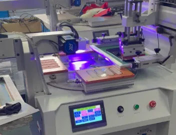
2. Direct Legend Printing (DLP)
Direct legend printing, often referred to as DLP, is a more advanced method that uses specialized inkjet printers to apply the silkscreen directly onto the PCB surface. Unlike traditional screen printing, DLP doesn’t require a stencil or mesh. Instead, the design is digitally transferred to the board, allowing for precise control over text size, placement, and detail.
Advantages:
- High precision, making it ideal for small text (down to 0.15 mm linewidths) and intricate designs.
- Faster setup since there’s no need for stencils or screens.
- Perfect for high-density boards where space is limited.
Limitations:
- Higher cost compared to traditional screen printing, especially for small runs.
- Specialized equipment is required, which may not be available at all fabrication facilities.
DLP is often the go-to choice for complex or miniaturized PCB designs where precision is critical. If your board includes fine details or tiny labels, this method ensures clarity and readability.
3. Liquid Photo Imaging (LPI)
Liquid photo imaging, or LPI, is a process similar to how solder masks are applied to PCBs. In this method, a liquid photo-imageable epoxy is coated onto the board. The desired silkscreen design is then exposed to UV light through a photomask, hardening the ink in specific areas. After exposure, the unhardened ink is washed away, and the remaining design is cured for durability.
Advantages:
- High accuracy and resolution, suitable for detailed markings.
- Consistent results across large production runs.
- Can be integrated with solder mask application for efficiency.
Limitations:
- More complex and time-consuming setup compared to screen printing.
- Higher cost due to the materials and equipment involved.
LPI is often used in professional settings where quality and consistency are paramount. It’s a reliable choice for medium to large production runs with moderately detailed silkscreen designs.
Step-by-Step Overview of the PCB Silkscreen Process
Regardless of the printing method, the PCB silkscreen process generally follows a few key steps. Understanding this workflow can help you design better silkscreens and communicate effectively with your fabrication team.
- Design Preparation: Create the silkscreen layer in your PCB design software, ensuring text, symbols, and logos are clear and properly placed. Common design rules include maintaining a minimum text height of 0.8 mm for readability and avoiding overlap with pads or vias.
- File Export: Export the silkscreen layer as part of your manufacturing files (often in Gerber format) and share it with your fabrication partner.
- Material Selection: Choose the ink color (typically white, yellow, or black) based on contrast with the board’s solder mask. White ink on a green or blue mask is a common choice for visibility.
- Application: Depending on the chosen method (screen printing, DLP, or LPI), the silkscreen is applied to the board’s surface.
- Curing: The ink is cured using heat or UV light to ensure it adheres permanently. This step typically takes around 10 minutes at high temperatures (e.g., 150°C) for most epoxy inks.
- Inspection: The board is inspected for alignment, clarity, and defects in the silkscreen layer before moving to assembly.
Following these steps ensures that your silkscreen is accurate and functional, reducing the risk of errors during assembly or testing.
Design Considerations for Effective PCB Silkscreen
Creating a useful silkscreen isn’t just about choosing the right printing method; it also requires thoughtful design. Here are some key considerations to keep in mind when designing your PCB silkscreen:
- Text Size and Readability: Use a minimum text height of 0.8 mm to ensure readability, especially for manual assembly or inspection. For DLP, you can go as low as 0.15 mm if necessary, but avoid overcrowding.
- Placement: Place markings near the relevant components or test points without overlapping critical areas like pads or traces. Ensure there’s at least 0.2 mm clearance from solderable areas to prevent interference.
- Color and Contrast: Choose an ink color that contrasts well with the solder mask. For example, white ink on a green mask provides excellent visibility, while black ink might work better on lighter masks.
- Content: Include essential information like component designators (e.g., R1 for a resistor), polarity indicators for diodes, and test point labels. Avoid clutter by prioritizing critical data over decorative elements.
- Orientation: Align text and symbols consistently for ease of reading. For instance, ensure all component labels are oriented in the same direction to avoid confusion during assembly.
By adhering to these guidelines, you can create a silkscreen that enhances functionality and minimizes errors during production and use.
Benefits of a Well-Designed Silkscreen
Investing time and effort into your PCB silkscreen design pays off in several ways:
- Improved Assembly Accuracy: Clear markings reduce the chances of misplaced components, saving time and costs during production.
- Easier Troubleshooting: Technicians can quickly identify test points and components, speeding up debugging and repairs.
- Professional Appearance: A polished silkscreen with logos and branding enhances the overall look of your product.
- Signal Integrity Protection: Proper placement of silkscreen markings avoids interference with critical areas, maintaining impedance control (e.g., avoiding discontinuities that could affect signals at high frequencies like 1 GHz).
Challenges and Solutions in PCB Silkscreen Printing
While the PCB silkscreen process is essential, it comes with potential challenges. Here are some common issues and how to address them:
- Overcrowding: On densely populated boards, there’s often not enough space for all desired markings. Solution: Prioritize critical labels and use smaller text sizes with high-precision methods like DLP.
- Ink Smudging or Peeling: Poor curing or low-quality ink can lead to durability issues. Solution: Work with a reliable fabrication partner who uses high-quality, non-conductive epoxy inks and proper curing techniques.
- Misalignment: Incorrect alignment during printing can render markings useless. Solution: Double-check design files and ensure precise registration during the printing process.
Choosing the Right Silkscreen Printing Method for Your Project
Selecting the best PCB silkscreen printing method depends on your project’s specific needs. Consider the following factors:
- Budget: If cost is a primary concern, traditional screen printing is often the most economical choice for larger runs.
- Design Complexity: For intricate designs or tiny text, opt for direct legend printing or liquid photo imaging for better resolution.
- Production Volume: High-volume runs may benefit from LPI due to its consistency, while small batches or prototypes might be better suited to DLP for faster setup.
- Board Density: High-density boards with limited space require precise methods like DLP to ensure readable markings.
Discussing your requirements with your fabrication partner can also help you make an informed decision tailored to your project.
Conclusion: Mastering the PCB Silkscreen Process
The PCB silkscreen process is a small but critical part of printed circuit board design and manufacturing. Whether you choose traditional screen printing, direct legend printing, or liquid photo imaging, understanding the strengths and limitations of each method ensures that your silkscreen serves its purpose—guiding assembly, aiding troubleshooting, and enhancing the professional look of your board. By focusing on thoughtful design, clear markings, and the right printing technique, you can avoid common pitfalls and create PCBs that are both functional and visually appealing.
At ALLPCB, we’re committed to supporting engineers and designers at every step of the PCB fabrication journey. With expertise in all PCB silkscreen printing methods, we’re here to help you achieve the best results for your projects. Dive into the world of silkscreen design with confidence, knowing that you have the tools and knowledge to succeed.


