 ALLPCB


In the fast-paced world of electronics design, PCB schematic design software has evolved far beyond simple drafting tools. For engineers and designers looking to tackle complex projects, advanced schematic design features like hierarchical schematics, variant management, integrated simulation, and collaboration tools in PCB design are game-changers. These features streamline workflows, reduce errors, and enable teams to create cutting-edge products with efficiency. In this blog, we’ll dive deep into these advanced capabilities, exploring how they enhance the design process and empower you to build better circuits.
Why Advanced Schematic Design Features Matter
As PCB designs grow in complexity, basic tools often fall short. Modern electronics, from high-speed communication devices to intricate IoT systems, demand precision and scalability. Advanced features in schematic design software address these needs by offering structured design approaches, error prevention, and team-friendly workflows. Whether you’re managing multiple design variants or simulating a circuit’s behavior before prototyping, these tools save time and resources. Let’s explore each feature in detail to understand their impact on your projects.
Hierarchical Schematics: Organizing Complexity with Ease
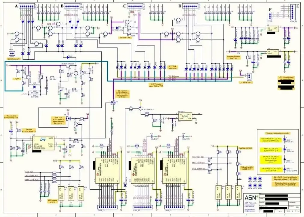
Hierarchical schematics are a cornerstone of advanced schematic design features, especially for large and intricate projects. This approach allows you to break down a design into smaller, manageable blocks or sheets, organized in a parent-child structure. Instead of cramming hundreds of components onto a single page, you can create a top-level schematic that links to detailed sub-sheets for specific circuit sections, like power supplies or signal processing units.
The benefits are clear. First, it improves readability, making it easier to navigate through a design with thousands of connections. For instance, in a multi-board system for a 5G communication device, a hierarchical setup lets you separate RF, digital, and power sections into distinct sheets. Second, it reduces errors by isolating changes to specific blocks without affecting the entire design. If you update a sub-sheet for a voltage regulator outputting 3.3V, the top-level schematic remains untouched.
Moreover, hierarchical designs support reusability. You can copy a block, like an amplifier circuit with a specific gain of 10 dB, across multiple projects without redrawing it each time. This saves hours of work and ensures consistency. For engineers working on scalable designs, this feature is indispensable for maintaining order in complexity.
Variant Management: Handling Multiple Design Configurations
In today’s market, products often come in multiple versions to meet different customer needs or regional standards. Variant management, another key aspect of advanced schematic design features, allows you to create and manage these versions within a single design file. Imagine designing a smart home controller that has a basic model with core features and a premium model with added Wi-Fi and Bluetooth modules. Variant management lets you define these differences without duplicating the entire schematic.
This feature works by letting you assign specific components or parameters to each variant. For example, you might specify a 2.4 GHz antenna for one version and a dual-band 2.4/5 GHz antenna for another. The software then generates tailored bills of materials (BOMs) and assembly instructions for each variant, reducing the risk of mix-ups during manufacturing. This not only saves time but also cuts down on costly production errors.
Variant management shines in industries like automotive electronics, where a single control unit might have dozens of configurations based on vehicle models. By centralizing these variations, you maintain control over the design process while ensuring accuracy across all versions.
Integrated Simulation: Testing Before Building
One of the most powerful advanced features in PCB design software is integrated simulation. This capability lets you test your circuit’s behavior directly within the design environment, long before you send it for prototyping. By simulating electrical performance, you can identify issues like signal integrity problems or thermal hotspots early in the process.
For example, consider a high-speed design operating at 10 Gbps. Integrated simulation can model signal delays, crosstalk, and impedance mismatches—say, detecting a problematic 50-ohm trace that causes reflections. You can then adjust the layout or component values, like tweaking a termination resistor from 100 ohms to 75 ohms, to optimize performance. Similarly, thermal simulations can predict if a power transistor will overheat under a 5W load, allowing you to add heat sinks or revise the design.
The advantage here is cost and time savings. Physical prototyping can take weeks and cost thousands of dollars, especially for complex multilayer boards. Simulation reduces the number of iterations needed, ensuring your design is production-ready faster. For engineers focused on reliability, this feature is a must-have in any modern design tool.
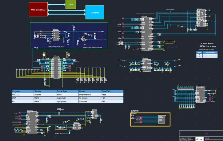
Collaboration Tools in PCB Design: Enhancing Teamwork
As projects grow in scale, teamwork becomes critical. Collaboration tools in PCB design software are advanced features that enable multiple engineers to work on the same project seamlessly, even if they’re in different locations. These tools include real-time design sharing, version control, and comment systems, ensuring everyone stays on the same page.
Imagine a team designing a medical device with strict regulatory requirements. One engineer focuses on the analog sensor circuit, while another handles the digital processing unit. Collaboration tools allow them to update their respective sections in real time, with changes instantly visible to the entire team. If a component like a 10 kΩ resistor is swapped for a 15 kΩ one, everyone sees the update, preventing conflicts or outdated designs.
Version control is another vital aspect. It tracks every change made to the schematic, so if a modification introduces an error—like a mismatched impedance of 75 ohms instead of 50 ohms—you can roll back to a previous version. Additionally, built-in commenting features let team members leave notes on specific design elements, fostering clear communication without endless email threads.
For distributed teams or companies with tight deadlines, collaboration tools in PCB design are essential for maintaining efficiency and quality. They bridge the gap between individual contributions and collective goals, ensuring smoother project delivery.
How These Features Transform Your Workflow
Combining hierarchical schematics, variant management, integrated simulation, and collaboration tools in PCB design creates a powerful ecosystem for tackling modern electronics challenges. Let’s look at a practical scenario: designing a modular IoT device with multiple configurations for different markets. Hierarchical schematics let you organize the design into blocks like power, connectivity, and sensors, making it easy to manage. Variant management ensures each market version, such as one with a 433 MHz module for Europe and a 915 MHz module for the US, is accurately defined. Integrated simulation verifies that signal timing meets a 100 ns threshold across all variants, while collaboration tools allow your global team to refine the design together.
The result? A streamlined process that cuts design time by up to 30%, reduces prototyping costs by avoiding errors, and ensures all team members contribute effectively. These advanced schematic design features don’t just add functionality—they transform how you approach projects, giving you the confidence to innovate without unnecessary risks.
Choosing the Right Software for Advanced PCB Design
Not all PCB design tools offer the full range of advanced features discussed here. When selecting software, prioritize those that support hierarchical schematics for complex projects, robust variant management for product diversity, integrated simulation for performance validation, and strong collaboration tools for team dynamics. Look for platforms with intuitive interfaces and comprehensive libraries to further speed up your workflow.
Additionally, consider scalability. As your projects grow, you’ll need software that can handle increasing complexity without performance lags. Check for compatibility with industry-standard formats like Gerber files for manufacturing, ensuring a smooth transition from design to production. By investing in a tool with these capabilities, you set yourself up for long-term success in creating reliable, high-performance electronics.
Conclusion: Elevate Your PCB Design with Advanced Tools
The landscape of PCB design is evolving, and staying ahead requires leveraging advanced schematic design features. Hierarchical schematics bring order to complexity, variant management simplifies multiple configurations, integrated simulation ensures reliability, and collaboration tools in PCB design empower teams to work smarter. Together, these capabilities help you create innovative, error-free designs faster and more cost-effectively.
At ALLPCB, we understand the importance of cutting-edge tools in bringing your ideas to life. By embracing software with these advanced features, you’re not just designing circuits—you’re building the future of electronics. Take the next step in your design journey and explore how these tools can elevate your projects to new heights.


