 ALLPCB


In the fast-paced world of electronics, designing printed circuit boards (PCBs) for high-speed signals is a critical skill. Whether you're working on cutting-edge communication devices or high-performance computing systems, mastering PCB design software for high-speed routing, impedance control, and signal integrity is essential. This guide dives deep into using advanced tools and techniques to ensure your designs handle high-speed signals with precision. From differential pair routing to crosstalk reduction in PCB design, we’ll explore how to optimize your workflow and achieve reliable results.
Why High-Speed PCB Design Matters
High-speed PCB design is crucial as modern electronics demand faster data transfer rates, often exceeding 1 GHz. These speeds introduce challenges like signal degradation, crosstalk, and electromagnetic interference (EMI). Without proper design techniques and software tools, your board may fail to perform, leading to costly redesigns or product failures. By leveraging specialized PCB design software for high-speed routing and signal integrity analysis tools, you can mitigate these risks and ensure your circuits operate flawlessly.
Key Challenges in High-Speed PCB Design
Designing for high-speed signals isn’t just about drawing traces on a board. It involves understanding and addressing several technical challenges:
- Signal Integrity: At high speeds, signals can distort due to reflections, delays, or noise. Maintaining signal integrity ensures data is transmitted without errors.
- Impedance Mismatches: Incorrect impedance can cause signal reflections. For example, a 50-ohm transmission line must match the source and load impedance to avoid issues.
- Crosstalk: When traces are too close, electromagnetic coupling can interfere with adjacent signals, especially at high frequencies.
- EMI: High-speed signals can emit or pick up interference, affecting performance and compliance with regulations.
Advanced PCB design software offers tools to tackle these challenges, ensuring your board performs reliably even at multi-gigabit speeds.
Choosing the Right PCB Design Software for High-Speed Routing
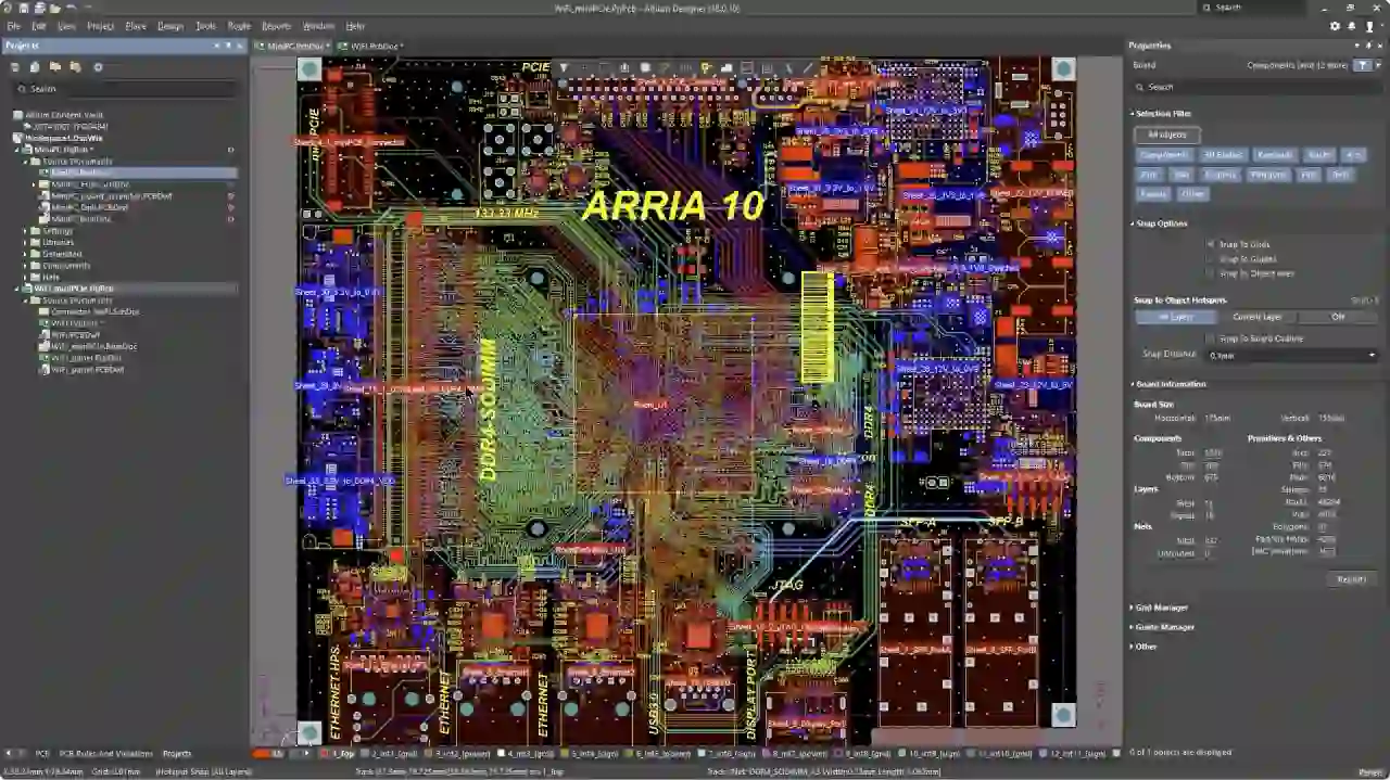
Selecting the right PCB design software for high-speed routing is the foundation of a successful design. Look for software that supports advanced features tailored to high-speed applications. These include automated routing for differential pairs, impedance calculators, and simulation capabilities for signal integrity analysis. Such tools help streamline the design process, saving time and reducing errors.
Modern software often includes libraries of predefined stack-ups and materials to help you achieve specific impedance values, such as 50 ohms for RF signals or 100 ohms for differential pairs. Additionally, many platforms provide real-time design rule checks (DRC) to flag issues like improper trace spacing or length mismatches during the layout phase.
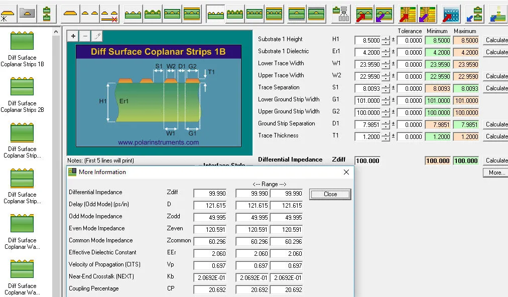
Mastering Impedance Control with Specialized Software
Impedance control is a cornerstone of high-speed PCB design. Mismatched impedance can lead to signal reflections, causing data errors or timing issues. Impedance control software integrated into PCB design platforms allows you to define trace width, spacing, and dielectric properties to achieve the desired impedance.
For instance, a common target for USB 3.0 differential pairs is 90 ohms. Using impedance control software, you can input parameters like trace thickness (typically 1 oz copper, or 35 μm), dielectric constant (often 4.2 for FR-4 material), and layer stack-up to calculate the exact trace width and spacing needed. Many tools also simulate how changes in these parameters affect impedance, helping you fine-tune your design before manufacturing.
By maintaining consistent impedance across your board, you minimize reflections and ensure signals travel smoothly from source to destination.
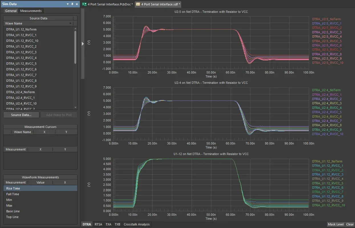
Signal Integrity Analysis Tools: Your Key to Reliable Designs
Signal integrity analysis tools are indispensable for high-speed PCB design. These tools simulate how signals behave on your board, identifying potential issues like overshoot, undershoot, or ringing. By running simulations before fabrication, you can catch and fix problems early, saving time and cost.
For example, signal integrity analysis can reveal if a 2.5 GHz signal experiences excessive jitter due to a poorly routed trace. Many software packages allow you to model transmission lines, terminations, and vias to predict signal behavior. Some even integrate with SPICE simulators to analyze both analog and digital components in your design.
Using these tools, you can test different routing strategies and stack-up configurations to optimize performance. This proactive approach ensures your board meets stringent timing and noise requirements, especially for applications like DDR4 memory or PCIe interfaces.
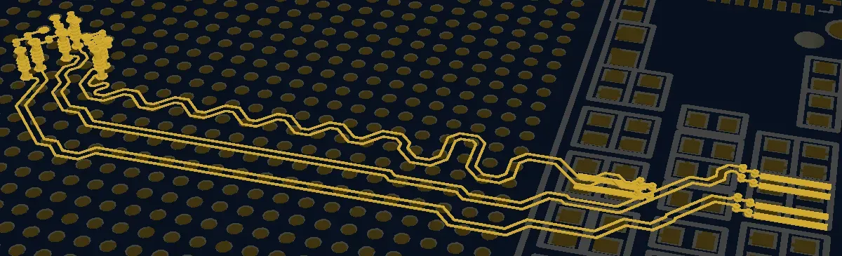
Differential Pair Routing for High-Speed Signals
Differential pair routing in PCB design is a technique used for high-speed signals like USB, HDMI, or Ethernet. Differential pairs consist of two traces carrying complementary signals, where noise affecting both traces equally is canceled out. This makes them ideal for maintaining signal integrity in noisy environments.
Effective differential pair routing requires precise length matching and consistent spacing. For instance, a length mismatch of just 5 mm in a 5 GHz signal can introduce skew, leading to data errors. PCB design software often includes automated tools to route differential pairs with matched lengths and controlled impedance, such as 100 ohms for many high-speed standards.
Additionally, keep differential pairs away from other traces to avoid crosstalk. Many design platforms allow you to set clearance rules to maintain a safe distance, ensuring minimal interference. By following these practices, you can achieve clean signal transmission even at high data rates.
Crosstalk Reduction in PCB Design: Strategies and Tools
Crosstalk reduction in PCB design is vital for high-speed circuits, as unwanted coupling between traces can corrupt signals. Crosstalk becomes more pronounced at higher frequencies, where even small electromagnetic fields can interfere with nearby traces.
Here are some proven strategies to minimize crosstalk, supported by modern PCB design software:
- Trace Spacing: Increase the distance between adjacent traces. A general rule is to maintain a spacing of at least 3 times the trace width (3W rule) to reduce coupling.
- Ground Planes: Use continuous ground planes beneath signal layers to shield traces from interference. Software can help you verify ground plane coverage during layout.
- Orthogonal Routing: Route traces on adjacent layers perpendicular to each other to minimize overlap and coupling.
- Guard Traces: Place grounded traces between high-speed signals to act as barriers against crosstalk. Many tools allow you to automate guard trace placement.
By applying these techniques and using software features to enforce design rules, you can significantly reduce crosstalk and improve overall board performance.
Best Practices for High-Speed PCB Design
Beyond specific tools and techniques, following best practices ensures your high-speed PCB design succeeds. Here are some actionable tips:
- Optimize Layer Stack-Up: Design your stack-up to include ground and power planes adjacent to signal layers for better shielding and impedance control. For a 4-layer board, a common configuration is signal-ground-power-signal.
- Minimize Via Usage: Vias introduce impedance discontinuities. Use them sparingly in high-speed paths, and opt for back-drilling in multilayer boards to reduce stub effects.
- Proper Termination: Use termination resistors (e.g., 50 ohms for RF lines) to match impedance and prevent reflections.
- Simulate Early and Often: Run signal integrity simulations at multiple stages of design to catch issues before they become costly problems.
Many PCB design platforms integrate these best practices into their workflows, offering wizards and templates to guide you through complex designs.
Advanced Features to Look for in PCB Design Software
As high-speed designs become more complex, advanced software features can make a significant difference. Here are some capabilities to prioritize:
- 3D Visualization: View your board in 3D to check for physical interference and ensure proper component placement near high-speed traces.
- EMI Simulation: Analyze potential electromagnetic interference to ensure compliance with standards like FCC or CE.
- Thermal Analysis: High-speed components often generate heat. Software with thermal simulation helps identify hotspots and optimize cooling.
- Design Collaboration: Cloud-based tools allow teams to collaborate on complex designs, ensuring consistency across revisions.
These features, combined with core functionalities like impedance control and differential pair routing, equip you to handle the most demanding high-speed projects.
Conclusion: Elevate Your High-Speed PCB Designs
Mastering PCB design software for high-speed signals takes your projects beyond basic schematics into the realm of cutting-edge electronics. By focusing on tools for high-speed routing, impedance control software, and signal integrity analysis, you can tackle the challenges of modern circuit design with confidence. Techniques like differential pair routing and crosstalk reduction in PCB design further ensure your boards perform reliably, even at gigabit speeds.
Invest time in learning the advanced features of your chosen software, and apply best practices to every layer of your design. With the right tools and strategies, you’ll create PCBs that meet the demands of today’s high-speed applications, delivering performance and reliability in equal measure.


