 ALLPCB


Why Embedded Passives Matter in Modern PCB Design
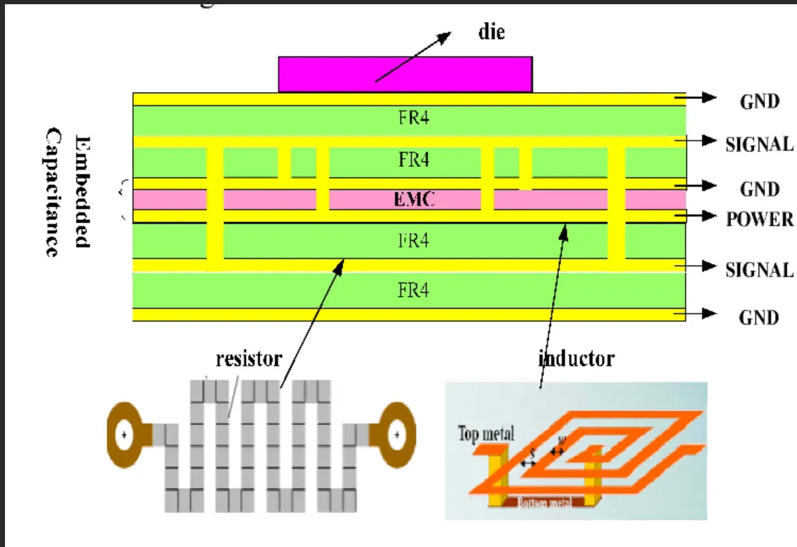
Embedded passives integrate passive components within the internal layers of a printed circuit board rather than mounting them on the surface. This placement shortens the paths between components and reduces the physical length of connections. In high-frequency PCB design, shorter paths help minimize parasitic inductance and capacitance that can distort signals. Engineers often turn to this method when discrete components introduce excessive variability or when board space becomes limited. The approach aligns with the need for consistent electrical behavior across operating frequencies.
Industry standards such as IPC-6012E guide the qualification of rigid printed boards that incorporate such features. These guidelines ensure that embedded elements meet performance criteria without compromising board integrity. As operating speeds rise, the relevance of embedded passives grows because they directly support cleaner signal transmission.
Technical Principles Behind Signal Integrity Improvements
Parasitic effects arise primarily from the leads, pads, and mounting structures of surface-mounted components. These elements add unwanted inductance and capacitance that alter impedance and create reflections or ringing on signal lines. Embedded passives eliminate much of this by placing the functional material directly within the dielectric layers. The reduced loop area lowers parasitic inductance, which proves especially beneficial at frequencies above several hundred megahertz.
Impedance control becomes more precise because the embedded elements can be positioned closer to the signal traces they serve. This proximity allows designers to maintain tighter tolerances on characteristic impedance throughout the board. In addition, the absence of surface discontinuities reduces the potential for electromagnetic interference coupling between adjacent traces. Thermal and mechanical stresses during operation also affect performance less severely when components reside inside the laminate structure.
Manufacturing processes must account for the integration steps, including material selection and layer registration accuracy. Standards such as IPC-A-600K provide acceptability criteria that help verify the quality of these internal features after fabrication.
Related Reading: Space-Saving Secrets: Designing Dense PCBs with Embedded Passives
Best Practices for Implementing Embedded Passives
Designers begin by evaluating which passive values lend themselves to embedding, typically focusing on resistors and capacitors in the lower ranges. Simulation tools model the expected parasitic reduction and confirm that target impedance values remain stable across the frequency range of interest. Material choices for the embedded layers require careful matching with the surrounding laminate to avoid mismatches in coefficient of thermal expansion.
During layout, placement rules emphasize proximity to active devices while respecting minimum spacing requirements for manufacturability. Via structures that connect to embedded elements should be minimized or optimized to further limit inductance. Collaboration between design and fabrication teams ensures that the chosen embedding technology aligns with available process capabilities.
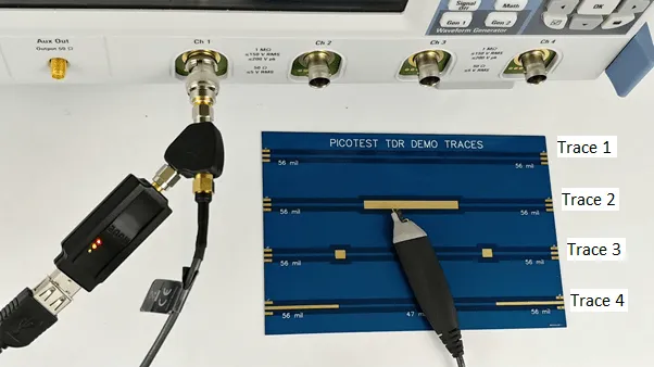
Testing protocols focus on both DC characteristics and high-frequency behavior. Time-domain reflectometry and network analysis verify that signal integrity targets are achieved. Iterative adjustments to layer stack-up or material properties often refine performance before final production release.
Practical Considerations in High-Frequency Applications
In applications such as telecommunications and computing hardware, embedded passives contribute to overall system reliability by lowering the risk of signal degradation over time. The technique also supports higher component density on the outer layers, freeing surface area for active devices or connectors. Engineers evaluate trade-offs between embedding density and yield expectations during the planning phase.
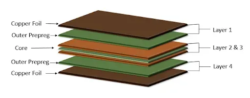
Process controls during lamination and curing steps help maintain the electrical properties of the embedded materials. Variations in thickness or alignment can shift the effective capacitance or resistance values, so monitoring these parameters remains essential. When properly executed, the resulting boards exhibit more predictable behavior under varying environmental conditions.
Related Reading: Embedded Components in PCB Design: Innovations and Use Cases
Conclusion
Embedded passives provide a direct method for enhancing signal integrity by addressing parasitic effects at their source. Through careful design and adherence to established qualification practices, engineers achieve improved impedance control and more stable high-frequency performance. The technique integrates seamlessly into existing PCB workflows when material and process considerations receive proper attention. Continued refinement of these methods supports the ongoing demands of advanced electronic systems.
FAQs
Q1: How do embedded passives improve signal integrity compared with discrete components?
A1: Embedded passives reduce parasitic inductance and capacitance by eliminating long leads and surface mounting structures. This results in cleaner signal transmission and better impedance control in high-frequency PCB design. The shorter current paths minimize reflections and ringing that can degrade performance.
Q2: What role does impedance control play when using embedded passives?
A2: Impedance control ensures that signal traces maintain consistent characteristic impedance along their length. Embedded passives support this goal by allowing precise placement near the traces they serve. Reduced parasitic effects help keep impedance within target tolerances across the operating frequency range.
Q3: Are there manufacturing considerations specific to embedded passives in PCBs?
A3: Yes, layer registration accuracy and material compatibility become critical during lamination. Process controls must verify that embedded resistor and capacitor values remain within specification after fabrication. Standards such as IPC-6012E outline qualification requirements that address these aspects.
Q4: When should designers consider embedded passives for PCB performance optimization?
A4: Designers evaluate embedded passives when surface-mounted components introduce unacceptable parasitic effects or when board space constraints limit layout options. The approach suits high-frequency applications where maintaining signal integrity is a primary requirement.
References
IPC-6012E — Qualification and Performance Specification for Rigid Printed Boards. IPC, 2017
IPC-A-600K — Acceptability of Printed Boards. IPC, 2020
JEDEC J-STD-020E — Moisture/Reflow Sensitivity Classification. JEDEC, 2014





